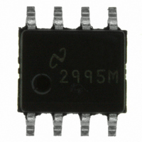
LP2995M/NOPB National Semiconductor, LP2995M/NOPB Datasheet

LP2995M/NOPB
Specifications of LP2995M/NOPB
LP2995M
Related parts for LP2995M/NOPB
LP2995M/NOPB Summary of contents
Page 1
... SENSE lation and a V output as a reference for the chipset and REF DDR DIMMS. Patents Pending Typical Application Circuit © 2011 National Semiconductor Corporation LP2995 Features ■ Low output voltage offset ■ Works with +5v, +3.3v and 2.5v rails ■ ...
Page 2
Connection Diagrams SO-8 (M08A) Package Top View PSOP-8 (MRA08A) Package Top View Pin Descriptions SO-8 Pin or PSOP-8 LLP Pin Pin 1 1,3,4,6,9, 13, 11 14, 15 ...
Page 3
... Absolute Maximum Ratings If Military/Aerospace specified devices are required, please contact the National Semiconductor Sales Office/ Distributors for availability and specifications. AVIN to GND PVIN to GND VDDQ (Note 2) Storage Temp. Range Junction Temperature PSOP-8 Thermal Resistance (θ Electrical Characteristics apply over the full Operating Temperature Range (T AVIN = PVIN = 2 ...
Page 4
Typical Performance Characteristics (25° (0, 25, 85, and 125° Temperature (No Load) REF www.national.com Iq vs Temperature ( V 20039309 20039311 OUT 20039313 4 = 2.5V) ...
Page 5
OUT Maximum Output Current (Sinking (VDDQ = 2.5) Maximum Output Current (Sourcing (VDDQ = 2.5) 20039315 IN 20039317 5 IN 20039316 www.national.com ...
Page 6
Block Diagram Description The LP2995 is a linear bus termination regulator designed to meet the JEDEC requirements of SSTL-2 and SSTL-3. The LP2995 is capable of sinking and sourcing current at the out- put V , regulating the voltage to ...
Page 7
Pin Descriptions AVIN AND PVIN AVIN and PVIN are the input supply pins for the LP2995. AVIN is used to supply all the internal control circuitry for the two op-amps and the output stage PVIN is used ...
Page 8
Thermal Dissipation Since the LP2995 is a linear regulator any current flow from V will result in internal power dissipation generating heat prevent damaging the part from exceeding the maximum allowable junction temperature, care should be taken to ...
Page 9
Typical Application Circuits The typical application circuit used for SSTL-2 termination schemes with DDR-SDRAM can be seen in For SSTL-3 and other applications it may be desirable to change internal reference voltage scaling from VDDQ * 0.5. An external resistor ...
Page 10
PCB Layout Considerations 1. AVIN and PVIN should be tied together for optimal performance. A local bypass capacitor should be placed as close as possible to the PVIN pin. 2. GND should be connected to a ground plane with multiple ...
Page 11
Physical Dimensions inches (millimeters) unless otherwise noted 8-Lead Small Outline Package (M8) NS Package Number M08A 11 www.national.com ...
Page 12
LLP Package (LD) NS Package Number LQA16A 8-Lead PSOP Package (PSOP-8) NS Package Number MRA08A 12 ...
Page 13
Notes 13 www.national.com ...
Page 14
... For more National Semiconductor product information and proven design tools, visit the following Web sites at: www.national.com Products Amplifiers www.national.com/amplifiers Audio www.national.com/audio Clock and Timing www.national.com/timing Data Converters www.national.com/adc Interface www.national.com/interface LVDS www.national.com/lvds Power Management www.national.com/power Switching Regulators www.national.com/switchers LDOs www.national.com/ldo LED Lighting www ...


