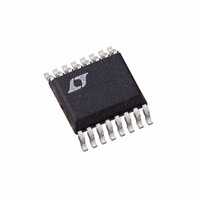
LTC3717EGN Linear Technology, LTC3717EGN Datasheet

LTC3717EGN
Specifications of LTC3717EGN
Available stocks
Related parts for LTC3717EGN
LTC3717EGN Summary of contents
Page 1
... Wide supply range allows operation from 4V to 36V at the V input LTC and LT are registered trademarks of Linear Technology Corporation trademark of Linear Technology Corporation. SENSE QDR RAMs and Quad Data Rate RAMs comprise a new family of products developed by Cypress Semiconductor, Hitachi, IDT, Micron Technology, Inc ...
Page 2
... REF 1V 50mV RNG FB REF 0V 50mV RNG FB REF INTV , RNG CC FB REF/2 RUN/SS Pin Rising RUN/SS Pin Falling U W ORDER PART NUMBER TOP VIEW 1 16 BOOST LTC3717EGN PGND INTV CC GN PART MARKING 8 9 EXTV CC 3717 GN PACKAGE 16-LEAD PLASTIC SSOP = 125 C, = 130 MIN ...
Page 3
... PGOOD Low Voltage PGL Note 1: Absolute Maximum Ratings are those values beyond which the life of a device may be impaired. Note calculated from the ambient temperature T J dissipation P as follows: D LTC3717EGN • 130 C/ The denotes specifications which apply over the full operating = 15V unless otherwise noted ...
Page 4
LTC3717 W U TYPICAL PERFOR A CE CHARACTERISTICS Efficiency vs Load Current 100 1.25V OUT FIGURE 1 CIRCUIT 0 0.01 0 100 LOAD ...
Page 5
W U TYPICAL PERFOR A CE CHARACTERISTICS INTV Load Regulation CC 0 –0.1 –0.2 –0.3 –0.4 –0 INTV LOAD CURRENT (mA) CC 3717 G14 Undervoltage Lockout Threshold vs Temperature 4.0 3.5 3.0 2.5 2.0 ...
Page 6
LTC3717 CTIO S RUN/SS (Pin 1): Run Control and Soft-Start Input. A capacitor to ground at this pin sets the ramp time to full output current (approximately 3s/ F) and the time delay for overcurrent ...
Page 7
CTIO AL DIAGRA 0. (10pF ION S Q 20k + + I CMP – – 1.4V V RNG 3 0.7V 5 240k Q2 I THB ...
Page 8
LTC3717 U OPERATIO Main Control Loop The LTC3717 is a current mode controller for DC/DC step-down converters. In normal operation, the top MOSFET is turned on for a fixed interval determined by a one-shot timer OST. When the top MOSFET ...
Page 9
U U APPLICATIO S I FOR ATIO the LTC3717 and external component values and a good guide for selecting the sense resistance is: V RNG R SENSE 10 • I OUT MAX ( ) An external resistive divider from INTV ...
Page 10
LTC3717 U U APPLICATIO S I FOR ATIO on-time t of the top MOSFET switch. The on-time is set ON by the current into the I pin according to ...
Page 11
U U APPLICATIO S I FOR ATIO current ratings from capacitor manufacturers are often based on only 2000 hours of life which makes it advisable to derate the capacitor. The selection primarily determined by the ESR OUT ...
Page 12
LTC3717 U U APPLICATIO S I FOR ATIO time that the LTC3717 is capable of turning on the bottom MOSFET, tripping the current comparator and turning the MOSFET back off. This time is generally about 300ns. The minimum off-time limit ...
Page 13
U U APPLICATIO S I FOR ATIO When the voltage on RUN/SS reaches 1.5V, the LTC3717 begins operating with a clamp on I 0.9V. As the RUN/SS voltage rises to 3V, the clamp raised until its full ...
Page 14
LTC3717 U U APPLICATIO S I FOR ATIO efficiency source, such as an output derived boost net- work or alternate supply if available loss. The input capacitor has the difficult job of IN filtering the large RMS input ...
Page 15
U U APPLICATIO S I FOR ATIO (This is typically the case, since V another DC/DC converter.) The ripple voltage will be only (ESR) OUT(RIPPLE) L(MAX) = (4A) (0.013 ) = 52mV However 10A ...
Page 16
LTC3717 U U APPLICATIO S I FOR ATIO • Flood all unused areas on all layers with copper. Flood- ing with copper will reduce the temperature rise of power component. You can connect the copper areas to any DC net ...
Page 17
U TYPICAL APPLICATIO 0 100k 11k 39k 680pF C 20k 100pF ...
Page 18
LTC3717 U TYPICAL APPLICATIO 0 100k 470pF C 20k 100pF 510k 2200pF ...
Page 19
... FLASH SHALL NOT EXCEED 0.010" (0.254mm) PER SIDE Information furnished by Linear Technology Corporation is believed to be accurate and reliable. However, no responsibility is assumed for its use. Linear Technology Corporation makes no represen- tation that the interconnection of its circuits as described herein will not infringe on existing patent rights. ...
Page 20
... Dual, Step-Down Controller LTC1876 2-Phase, Dual Synchronous Step-Down Controller with Step-Up Regulator LTC3413 Monolithic DDR Memory Termination Regulator Burst Mode is a registered trademark of Linear Technology Corporation. Linear Technology Corporation 20 1630 McCarthy Blvd., Milpitas, CA 95035-7417 (408) 432-1900 FAX: (408) 434-0507 Typical Application 1.25V 1.4MHz ...


