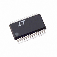
LTC3714EG#TR Linear Technology, LTC3714EG#TR Datasheet - Page 16

LTC3714EG#TR
Manufacturer Part Number
LTC3714EG#TR
Description
IC STP-DWN CNTRLR W/OPAMP 28SSOP
Manufacturer
Linear Technology
Datasheet
1.LTC3714EGPBF.pdf
(22 pages)
Specifications of LTC3714EG#TR
Applications
Controller, Intel Pentium®
Voltage - Input
4 ~ 36 V
Number Of Outputs
1
Voltage - Output
0.6 ~ 1.75 V
Operating Temperature
-40°C ~ 85°C
Mounting Type
Surface Mount
Package / Case
28-SSOP
Lead Free Status / RoHS Status
Contains lead / RoHS non-compliant
Other names
LTC3714EGTR
Available stocks
Company
Part Number
Manufacturer
Quantity
Price
applicaTions inForMaTion
LTC3417A
Remembering that the above junction temperature is
obtained from an R
the junction temperature based on a higher R
it increases with temperature. However, we can safely as-
sume that the actual junction temperature will not exceed
the absolute maximum junction temperature of 125°C.
Design Example
As a design example, consider using the LTC3417A in
a portable application with a Li-Ion battery. The battery
provides a V
at 1.5A in active mode, and 1mA in standby mode. The
other load requires 2.5V at 1A in active mode, and 500µA
in standby mode. Since both loads still need power in
standby, Burst Mode operation is selected for good low
load efficiency (SYNC/MODE = V
First, determine what frequency should be used. Higher
frequency results in a lower inductor value for a given ∆I
(∆I
for wire wound surface mount inductors are usually in the
range of 1µH to 10µH.
Using the 1.5MHz frequency setting (FREQ = V
the following equations for L1 and L2:
16
CONVERTER OUTPUT
L1=
Use 1.5µH.
L2 =
Use 2.2µH.
L
is estimated as 0.35I
1.5MHz • 525mA
1.5MHz • 350mA
SW1
SW2
IN
1.8V
2.5V
from 2.8V to 4.2V. One load requires 1.8V
DS(ON)
LOAD(MAX)
⎛
⎜
⎝
⎛
⎜
⎝
at 25°C, we might recalculate
1–
I
1–
LOAD(MAX)
1.5A
1A
1.8V
4.2V
2.5V
4.2V
IN
).
). Reasonable values
⎞
⎟ = 1.3µH
⎠
⎞
⎟ = 1.9µH
⎠
DS(ON)
525mA
350mA
IN
∆I
), we get
L
since
L
C
requirements. For a 2.5% output droop:
The closest standard values are 47µF and 22µF .
The output voltages can now be programmed by choos-
ing the values of R1, R2, R3, and R4. To maintain high
efficiency, the current in these resistors should be kept
small. Choosing 2µA with the 0.8V feedback voltages makes
R2 and R4 equal to 400k. A close standard 1% resistor is
412k. This then makes R1 = 515k. A close standard 1%
is 511k. Similarily, with R4 at 412k, R3 is equal to 875k.
A close 1% resistor is 866k.
The compensation should be optimized for these com-
ponents by examining the load step response, but a
good place to start for the LTC3417A is with a 5.9kΩ and
2200pF filter on I
output capacitor may need to be increased depending on
the actual undershoot during a load step.
The PGOOD pin is a common drain output and requires a
pull-up resistor. A 100k resistor is used for adequate speed.
Figure 4 shows a complete schematic for this design.
OUT
C
C
OUT1
OUT2
selection is based on load step droop instead of ESR
= 2.5 •
= 2.5 •
1.5MHz 5% • 1.8V
TH1
1.5MHz 5% • 2.5V
and 2.87k and 6800pF on I
1.5A
(
(
1A
)
)
= 28µF
= 13µF
TH2
. The
3417afc


