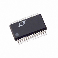
LTC3714EG#TRPBF Linear Technology, LTC3714EG#TRPBF Datasheet - Page 15

LTC3714EG#TRPBF
Manufacturer Part Number
LTC3714EG#TRPBF
Description
IC STP-DWN CNTRLR W/OPAMP 28SSOP
Manufacturer
Linear Technology
Datasheet
1.LTC3714EGPBF.pdf
(22 pages)
Specifications of LTC3714EG#TRPBF
Applications
Controller, Intel Pentium®
Voltage - Input
4 ~ 36 V
Number Of Outputs
1
Voltage - Output
0.6 ~ 1.75 V
Operating Temperature
-40°C ~ 85°C
Mounting Type
Surface Mount
Package / Case
28-SSOP
Lead Free Status / RoHS Status
Lead free / RoHS Compliant
Available stocks
Company
Part Number
Manufacturer
Quantity
Price
applicaTions inForMaTion
3) I
The R
be obtained from the Typical Performance Characteristics
curves. Thus, to obtain I
where R
4) Other “hidden” losses such as copper trace and internal
Thermal Considerations
The LTC3417A requires the package Exposed Pad
(PGND2/GNDD pin) to be well soldered to the PC board.
This gives the DFN and TSSOP packages exceptional
thermal properties, compared to similar packages of this
size, making it difficult in normal operation to exceed the
maximum junction temperature of the part. In a majority
low to high to low again, a packet of charge moves from
V
period is a current out of V
than the DC bias current. The gate charge losses are
proportional to V
pronounced at higher supply voltages.
internal switches, R
continuous mode, the average output current flowing
through inductor L is “chopped” between the internal
top and bottom switches. Thus, the series resistance
looking into the SW pin is a function of both top and
bottom MOSFET R
follows:
R
I
battery resistances can account for additional efficiency
degradations in portable systems. It is very important
to include these “system” level losses in the design
of a system. The internal battery and fuse resistance
losses can be minimized by making sure that C
adequate charge storage and very low ESR
the switching frequency. Other losses including diode
conduction losses during dead-time and inductor core
losses generally account for less than 2% total additional
loss.
2
2
IN
SW
R losses are calculated from the DC resistances of the
R losses = I
DS(ON)
to ground. The resulting charge over the switching
= (R
L
is the resistance of the inductor.
DS(ON)
for both the top and bottom MOSFETs can
OUT
TOP)(DC) + (R
IN
2
(R
DS(ON)
SW
and thus their effects will be more
SW
2
, and the external inductor, R
R losses:
+ R
IN
and the duty cycle (DC) as
that is typically much larger
L
)
DS(ON)
BOT)(1 – DC)
COUT
IN
L
has
. In
at
of applications, the LTC3417A does not dissipate much
heat due to its high efficiency. However, in applications
where the LTC3417A is running at high ambient tem-
perature with low supply voltage and high duty cycles,
such as in dropout, the heat dissipated may exceed the
maximum junction temperature of the part. If the junction
temperature reaches approximately 150°C, both switches
in both regulators will be turned off and the SW nodes will
become high impedance.
To prevent the LTC3417A from exceeding its maximum
junction temperature, the user will need to do some thermal
analysis. The goal of the thermal analysis is to determine
whether the power dissipated exceeds the maximum
junction temperature of the part. The temperature rise is
given by:
where P
is the thermal resistance from the junction of the die to
the ambient temperature.
The junction temperature, T
As an example, consider the case when the LTC3417A is
in dropout in both regulators at an input voltage of 3.3V
with load currents of 1.5A and 1A. From the Typical Per-
formance Characteristics graph of Switch Resistance, the
R
and the R
The power dissipated by the part is:
The DFN package junction-to-ambient thermal resistance,
θ
of the regulator operating in a 70°C ambient temperature
is approximately:
JA
DS(ON)
T
T
PD = I
PD = 1.5
PD = 366mW
T
T
, is about 43°C/W. Therefore, the junction temperature
RISE
J
J
J
= T
= 0.366 • 43 + 70
= 85.7°C
D
resistance of the 1.5A P-channel switch is 0.09Ω
= P
RISE
1
is the power dissipated by the regulator and θ
DS(ON)
2
2
• R
D
+ T
• 0.09 + 1
• θ
DS(ON)1
AMBIENT
JA
of the 1A P-channel switch is 0.163Ω.
+ I
2
• 0.163
2
2
J
• R
, is given by:
DS(ON)2
LTC3417A
15
3417afc
JA


