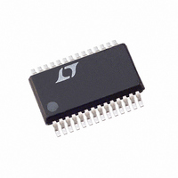
LTC3714EG#TRPBF Linear Technology, LTC3714EG#TRPBF Datasheet - Page 3

LTC3714EG#TRPBF
Manufacturer Part Number
LTC3714EG#TRPBF
Description
IC STP-DWN CNTRLR W/OPAMP 28SSOP
Manufacturer
Linear Technology
Datasheet
1.LTC3714EGPBF.pdf
(22 pages)
Specifications of LTC3714EG#TRPBF
Applications
Controller, Intel Pentium®
Voltage - Input
4 ~ 36 V
Number Of Outputs
1
Voltage - Output
0.6 ~ 1.75 V
Operating Temperature
-40°C ~ 85°C
Mounting Type
Surface Mount
Package / Case
28-SSOP
Lead Free Status / RoHS Status
Lead free / RoHS Compliant
Available stocks
Company
Part Number
Manufacturer
Quantity
Price
elecTrical characTerisTics
temperature range, otherwise specifications are at T
SYMBOL
I
f
I
I
R
R
I
I
V
T
R
V
V
I
I
I
VTL
VTH
VTH
Note 1: Stresses beyond those listed under Absolute Maximum Ratings
may cause permanent damage to the device. Exposure to any Absolute
Maximum Rating condition for extended periods may affect device
reliability and lifetime.
Note 2: The LTC3417AE is guaranteed to meet specified performance from
0°C to 85°C. Specifications over the –40°C to 85°C operating ambient
temperature range are assured by design, characterization and correlation
with statistical process controls. The LTC3417AI is guaranteed to meet
performance specifications over the –40°C to 85°C operating temperature
range.
Note 3: The LTC3417A is tested in feedback loop which servos V
midpoint for the error amplifier (V
the error amplifier (V
Note 4: Total supply current is higher due to the internal gate charge being
delivered at the switching frequency.
S
OSC
LIM1
LIM2
SW1(LKG)
SW2(LKG)
RUN1
PHASE
SYNC/MODE
PGOOD
UVLO
RUN1
PHASE
DS(ON)1
DS(ON)2
PGOOD
SYNC/MODE
SYNC/MODE
FREQ
, I
, V
,
RUN2
RUN2
,
PARAMETER
Input DC Supply Current (Note 4)
Oscillator Frequency
Peak Switch Current Limit on SW1 (1.5A)
Peak Switch Current Limit on SW2 (1A)
SW1 Top Switch On-Resistance (1.5A)
SW1 Bottom Switch On-Resistance
SW2 Top Switch On-Resistance (1A)
SW2 Bottom Switch On-Resistance
Switch Leakage Current SW1 (1.5A)
Switch Leakage Current SW2 (1A)
Undervoltage Lockout Threshold
Threshold for Power Good. Percentage
Deviation from V
(Typically 0.8V)
Power Good Pull-Down On-Resistance
RUN1, RUN2 Threshold
PHASE Threshold High-CMOS Levels
PHASE Threshold Low-CMOS Levels
RUN1, RUN2, PHASE and SYNC/MODE
Leakage Current
SYNC/MODE Threshold Voltage Low
SYNC/MODE Threshold Voltage High
FREQ Threshold Voltage High
Active Mode
Half Active Mode (V
Half Active Mode (V
Both Channels in Sleep Mode
Shutdown
ITH2
= 0.6V).
FB
ITH1
Steady State
RUN2
RUN1
= 0.6V) and V
= 0V, 1.5A Only)
= 0V, 1A Only)
FB2
to the midpoint for
A
= 25°C. V
FB1
CONDITIONS
The
V
V
V
V
V
V
V
V
V
V
V
V
V
V
V
V
V
V
V
V
V
V
to the
FB1
RUN1
FB1
FB2
FB1
RUN1
RUN1
FREQ
FREQ
FREQ
IN1
IN1
IN2
IN2
IN1
IN2
IN1
IN1
FB1
FB1
SYNC/MODE
IN
= 6V, V
, V
, V
= 3.6V (Note 5)
= 3.6V (Note 5)
= 3.6V (Note 5)
= 3.6V (Note 5)
= 6V, V
= 6V, V
l
= V
= 0.75V, V
= 0.75V, V
= V
or V
or V
IN
: R
: Resistor (Note 6)
= V
IN2
= V
= V
= V
IN2
denotes the specifications which apply over the full operating
= 3.6V unless otherwise specified. (Note 2)
FB2
FB2
T
FB2
FB2
IN
RUN2
RUN2
RUN2
Ramping Down
= 143k
Ramping Up
PVIN
ITH1
ITH2
= 0.75V, V
= 1V, V
= 0V
Note 5: Switch on-resistance is guaranteed by design and test correlation
on the DHC package and by final test correlation on the FE package.
Note 6: Variable frequency operation with resistor is guaranteed by design
but not production tested and is subject to duty cycle limitations.
Note 7: This IC includes overtemperature protection that is intended
to protect the device during momentary overload conditions. Junction
temperature will exceed 125°C when overtemperature protection is active.
Continuous operation above the specified maximum operating junction
temperature may impair device reliability.
Note 8: T
sipation, P
Ramping Up, V
Ramping Down,
SYNC/MODE
SYNC/MODE
= 3V
= V
= V
= 0V
LTC3417AEDHC: T
LTC3417AEFE: T
= 0V, V
= 0V, V
IN
IN
SYNC/MODE
J
SYNC/MODE
RUN1
RUN2
D
is calculated from the ambient temperature, T
, according to the following formula:
= V
= V
SYNC/MODE
= 0V
= 0V
IN
IN
= V
, V
, V
J
= V
IN
RUN1
RUN2
= T
J
,
= T
IN
A
,
+ (P
= 0V
= V
= V
A
+ (P
IN
IN
D
• 38°C/W)
D
• 43°C/W)
V
V
V
IN
IN
IN
0.85
1.95
MIN
1.2
2.1
1.4
1.9
0.3
–0.5
–0.5
–0.5
LTC3417A
0.088
0.084
0.16
0.15
0.01
0.01
2.07
2.12
0.85
0.01
TYP
400
260
260
125
160
0.1
1.5
2.5
1.7
–6
–6
1
A
, and power dis-
MAX
1.25
2.25
600
400
400
250
300
1.8
2.2
1.5
0.5
0.5
1
4
1
1
1
UNITS
3417afc
3
MHz
MHz
MHz
µA
µA
µA
µA
µA
µA
µA
µA
%
%
Ω
Ω
Ω
Ω
Ω
A
A
V
V
V
V
V
V
V
V


