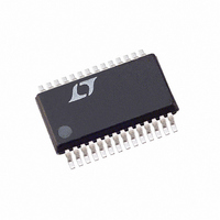
LTC3714EG#TRPBF Linear Technology, LTC3714EG#TRPBF Datasheet - Page 6

LTC3714EG#TRPBF
Manufacturer Part Number
LTC3714EG#TRPBF
Description
IC STP-DWN CNTRLR W/OPAMP 28SSOP
Manufacturer
Linear Technology
Datasheet
1.LTC3714EGPBF.pdf
(22 pages)
Specifications of LTC3714EG#TRPBF
Applications
Controller, Intel Pentium®
Voltage - Input
4 ~ 36 V
Number Of Outputs
1
Voltage - Output
0.6 ~ 1.75 V
Operating Temperature
-40°C ~ 85°C
Mounting Type
Surface Mount
Package / Case
28-SSOP
Lead Free Status / RoHS Status
Lead free / RoHS Compliant
Available stocks
Company
Part Number
Manufacturer
Quantity
Price
pin FuncTions
LTC3417A
RUN1 (Pin 1/Pin 2): Enable for 1.5A Regulator. When
at Logic 1, 1.5A regulator is running. When at 0V, 1.5A
regulator is off. When both RUN1 and RUN2 are at 0V,
the part is in shutdown.
V
1.5A Regulator.
I
for 1.5A Regulator. The current comparator threshold
increases with this control voltage. Nominal voltage range
for this pin is 0V to 1.5V.
V
external resistive divider across the 1.5A regulator output.
Nominal voltage for this pin is 0.8V.
V
external resistive divider across the 1A regulator output.
Nominal voltage for this pin is 0.8V.
I
1A regulator. The current comparator threshold increases
with this control voltage. Nominal voltage range for this
pin is 0V to 1.5V.
RUN2 (Pin 7/Pin 8): Enable for 1A Regulator. When at
Logic 1, 1A regulator is running. When at 0V, 1A regula-
tor is off. When both RUN1 and RUN2 are at 0V, the part
is in shutdown.
V
Regulator and Supply for Analog Circuitry.
SYNC/MODE (Pin 9/Pin 12): Combination Mode Selection
and Oscillator Synchronization Pin. This pin controls the op-
eration of the device. When the voltage on the SYNC/MODE
pin is >(V
When the voltage on the SYNC/MODE pin is <0.5V, pulse
skipping mode is selected. When the SYNC/MODE pin is
held at V
oscillation frequency can be synchronized to an external
6
TH1
TH2
IN1
FB1
FB2
IN2
(Pin 6/Pin 7): Error Amplifier Compensation Point for
(Pin 8/Pin 9): Supply Pin for P-Channel Switch of 1A
(Pin 3/Pin 4): Error Amplifier Compensation Point
(Pin 2/Pin 3): Supply Pin for P-Channel Switch of
(Pin 4/Pin 5): Receives the feedback voltage from
(Pin 5/Pin 6): Receives the feedback voltage from
IN
IN
/2, forced continuous mode is selected. The
– 0.5V), Burst Mode operation is selected.
(DFN/TSSOP)
oscillator applied to this pin. When synchronized to an
external clock, pulse skip mode is selected.
SW2 (Pin 10/Pin 13): Switch Node Connection to the
Inductor for the 1A Regulator. This pin swings from V
to PGND2.
PGOOD (Pin 11/Pin 14): Power Good Pin. This common
drain-logic output is pulled to GND when the output voltage
of either regulator is – 6% of regulation. If either RUN1 or
RUN2 is low (the respective regulator is in sleep mode and
therefore the output voltage is low), then PGOOD reflects
the regulation of the running regulator.
FREQ (Pin 12/Pin 15): Frequency Set Pin. When FREQ is
at V
is connected from this pin to ground, the internal oscillator
frequency can be varied from 0.6MHz to 4MHz.
GNDA (Pin 13/Pin 16): Analog Ground Pin for Internal
Analog Circuitry.
PHASE (Pin 14/Pin 17): Selects 1A regulator switching
phase with respect to 1.5A regulator switching. Set to V
the 1.5A regulator and the 1A regulator are in phase. When
PHASE is at 0V, the 1.5A regulator and the 1A regulator
are switching 180 degrees out-of-phase.
SW1 (Pin 15/Pin 18): Switch Node Connection to the
Inductor for the 1.5A Regulator. This pin swings from
V
PGND1 (Pin 16/Pin 19): Ground for SW1 N-Channel
Driver.
PGND2, GNDD (Pins 1,10,11,20): TSSOP Package Only.
Ground for SW2 N-channel driver and digital ground for
circuit.
Exposed Pad (Pin 17/Pin 21): PGND2, GNDD. Ground for
SW2 N-channel driver and digital ground for circuit. The
Exposed Pad must be soldered to PCB ground.
IN1
IN
to PGND1.
, internal oscillator runs at 1.5MHz. When a resistor
3417afc
IN2
IN
,


