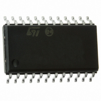
L5951 STMicroelectronics, L5951 Datasheet

L5951
Specifications of L5951
Available stocks
Related parts for L5951
L5951 Summary of contents
Page 1
... RX January 2001 GROUND OR BATTERY ESD PROTECTED DESCRIPTION The L5951 is a monolithic triple regulator integrated with a SAE J1850 Integrated Driver / Receiver real- ized in advanced Multipower-BCD technology intended to drive single wire J1850 communications, and offer microcontroller power and power manage- ment for automotive or industrial applications. ...
Page 2
... Low Input Voltage Operation - If battery voltage level drops below 7.0V, the outputs are to remain alive and ready for the return of normal voltage battery levels. The L5951 will be able to retrieve data off the BUS and send it to the micrprocessor when the supply voltage is as low as 4.9V. The regulators should stay the same voltage as the battery voltage down to 7 ...
Page 3
... Maximum Nodes 1.5 Protection The L5951 can survive under the following conditions: shorting the outputs to BAT and GND, loss of BAT, loss of IC GND, double battery(+26.5V), 4000V ESD, 34V load dump. L5951 will not handle a reverse battery con- dition. External components must be implemented for reverse battery protection. ...
Page 4
... L5951 high pulse identified by a pulse width of about t = 200 s. DATA - Total number of bytes that can be transmitted (from SOF to EOF bytes. Cyclic Redundancy Check (CRC method for determining if the message received is the same as the mes- sage transmitted invalid CRC number is detected, then an error will be detected. The SOF signal is not used to determine the CRC. All bits in the CRC are initially " ...
Page 5
... Low Voltage Supply *denotes active low for Sleep and Reset. REG1 1 24 RESET 2 23 REXT GND_TX 5 20 GND_TX 6 19 GND_TX 7 18 GND_TX 8 17 SLEEP LOOP 12 13 D99AU992 Function L5951 LVS REG2 REG3 BAT GND_TX GND_TX GND_TX GND_TX BUS LOAD TX RX 5/13 ...
Page 6
... L5951 ELECTRICAL CHARACTERISTICS (T = 25° 14.4V unless otherwise specified. Standard Loads: I amb BAT Symbol Parameter I Standby Quiescent Current q,ST-BY Maximum QuiescentCurrent - V BAT Maximum QuiescentCurrent - LVS EN Switch Input Current V EN Input Threshold Voltage ENL, ENH V Reset* Output Low Voltage RES Reset* Output Voltage Threshold ...
Page 7
... BUS = - VDC BUS = BAT I = 6mA LOAD = 0.5mA 0.5mA, I REG1 REG2 REG3 Min. Typ. Max. 14 LOAD 450 22 200 = 50mA 45 V 7.60 7.8 BAT BAT LOAD 0.5 0.04 200 = 50mA 45 4.25 3.7 3.50 0.15 to gnd 7.2 5 170 0 0 0.045 L5951 = 5mA) Unit 100 7/13 ...
Page 8
... L5951 ELECTRICAL CHARACTERISTICS (continued 25° 14.4V unless otherwise specified. Standard Loads: I amb BAT Symbol Parameter LOAD Load Output (Unpowered) Dio I BUS & LOADCurrent during loss BUSloss of assembly V or GND I BAT LOADloss TX TX Input Voltage VIL TX VIH I TX Input Current TXVIL I TXVIH ...
Page 9
... See Figure 5, Sleep* = 0VDC 64 sec TX BUS t rise t fall 64 sec TX 6.25V >35 sec 3.875V 64 sec 1.5V <93 sec = 0.5mA 0.5mA, I REG1 REG2 REG3 Min. Typ. Max. 100 80 16 3.5 14.5 1.5 1.9 170 70 170 70 6.25V 1.5V D99AU993 D99AU994 L5951 = 5mA) Unit 9/13 ...
Page 10
... L5951 Figure 3. BUS Output Voltage Figure 4. BUS to RX Delay Times 3 TYPICAL APPLICATION CURCUIT Figure 5. Application Circui VBATT C10 C1 470 F 0.1 F 10V C8 0.1 F FROM LOGIC TO LOGIC Note: ESR of output capacitors should be between 0.2 10/13 BUS ltoh 90% 90% RX 10% BAT 47K LVS SLEEP ...
Page 11
... Pull Down Resistor 4. Bus Resistor 5. Bus Slew Rate Control 6. Proper Bus Capacitance 5VSB R RESET to micro C D99AU999 Part Description CAP - 0.1 F, 25V CAP - Tant 10 F, 10V RES-47k, 1/16W 5% RES - 10.7k, 1/16W, 1% RES - 68k, 1/16W, 1% CAP - 25V, 470pF CAP - 50V, 470pF L5951 Note Number 11/13 ...
Page 12
... L5951 mm DIM. MIN. TYP. MAX. A 2.35 2.65 0.093 A1 0.10 0.30 0.004 A2 2.55 B 0.33 0.51 0.013 C 0.23 0.32 0.009 D 15.20 15.60 0.598 E 7.40 7.60 0.291 e 1.27 H 10.0 10.65 0.394 h 0.25 0.75 0.010 k 0 (min.), 8 (max.) L 0.40 1.27 0.016 B 0.10mm .004 Seating Plane ...
Page 13
... STMicroelectronics. The ST logo is a registered trademark of STMicroelectronics Australia - Brazil - China - Finland - France - Germany - Hong Kong - India - Italy - Japan - Malaysia - Malta - Morocco - Singapore - Spain 2001 STMicroelectronics - All Rights Reserved STMicroelectronics GROUP OF COMPANIES - Sweden - Switzerland - United Kingdom - U.S.A. http://www.st.com L5951 13/13 ...


