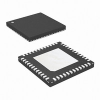
ISL6262CRZ Intersil, ISL6262CRZ Datasheet - Page 19

ISL6262CRZ
Manufacturer Part Number
ISL6262CRZ
Description
IC CORE REG 2PHASE 48-QFN
Manufacturer
Intersil
Datasheet
1.ISL6262CRZ.pdf
(27 pages)
Specifications of ISL6262CRZ
Applications
Converter, Intel IMVP-6
Voltage - Input
5 ~ 25 V
Number Of Outputs
1
Voltage - Output
0.3 ~ 1.5 V
Operating Temperature
-10°C ~ 100°C
Mounting Type
Surface Mount
Package / Case
48-VQFN
Lead Free Status / RoHS Status
Lead free / RoHS Compliant
Available stocks
Company
Part Number
Manufacturer
Quantity
Price
Company:
Part Number:
ISL6262CRZ
Manufacturer:
AMD
Quantity:
144
Part Number:
ISL6262CRZ
Manufacturer:
INTERSIL
Quantity:
20 000
SLEWRATE, as given in the IMVP-6 specification will
determine the choice of the SOFT capacitor, C
following equation:
Using a SLEWRATE of 10mV/µs, and the typical I
given in the Electrical Specification Table of 200µA, C
is
A choice of 0.015µF would guarantee a SLEWRATE of
10mV/µs is met for minimum I
Electrical Specification Table. This choice of C
control the Start-Up slewrate as well. One should expect the
output voltage to slew to the Boot value of 1.2V at a rate
given by the following equation:
Selecting RBIAS
To properly bias the ISL6262, a reference current is
established by placing a 147kΩ, 1% tolerance resistor from
the RBIAS pin to ground. This will provide a highly accurate,
10µA current source from which OCSET reference current
can be derived.
Care should be taken in layout that the resistor is placed
very close to the RBIAS pin and that a good quality signal
ground is connected to the opposite side of the RBIAS
resistor. Do not connect any other components to this pin as
this would negatively impact performance. Capacitance on
this pin would create instabilities and should be avoided.
Start-Up Operation - CLK_EN# and PGOOD
The ISL6262 provides a 3.3V logic output pin for CLK_EN#.
The 3V3 pin allows for a system 3.3V source to be
connected to separated circuitry inside the ISL6262, solely
devoted to the CLK_EN# function. The output is a 3.3V
CMOS signal with 4mA sourcing and sinking capability. This
implementation removes the need for an external pull-up
resistor on this pin, and due to the normal level of this signal
being a low, removes the leakage path from the 3.3V supply
to ground through the pull-up resistor. This reduces 3.3V
supply current, that would occur under normal operation with
a pull-up resistor, and prolongs battery life. The 3.3V supply
should be decoupled to digital ground, not to analog ground
for noise immunity.
As mentioned in the “Theory of Operation” section of this
datasheet, CLK_EN# is logic level high at start-up until 20µs
after the system Vccp and Vcc_mch supplies are within
regulation, and the Vcc-core is in regulation at the Boot level.
Approximately 20µs after these voltages are within
regulation, as indicated by PGD_IN going high, CLK_EN#
goes low, triggering an internal timer for the
C
C
dV
-------
dt
SOFT
SOFT
=
-------------------
C
SOFT
=
=
I
SS
----------------------------------- -
SLEWRATE
200μA
=
I
GV
---------------------- -
0.015μF
⁄
41μA
(
10mV 1μs
⁄
=
2.8mV μs
19
)
GV
value, given in the
⁄
SOFT
SOFT
GV
, by the
will then
value,
SOFT
(EQ. 1)
(EQ. 2)
(EQ. 3)
ISL6262
IMVP-6_PWRGD signal. This timer allows IMVP-6_PWRGD
to go high approximately 6.8ms after CLK_EN# goes low.
Static Mode of Operation - Processor Die Sensing
Die sensing is the ability of the controller to regulate the core
output voltage at a remotely sensed point. This allows the
voltage regulator to compensate for various resistive drops
in the power path and ensure that the voltage seen at the
CPU die is the correct level independent of load current.
The VSEN and RTN pins of the ISL6262 are connected to
Kelvin sense leads at the die of the processor through the
processor socket. These signal names are Vcc_sense and
Vss_sense respectively. This allows the voltage regulator to
tightly control the processor voltage at the die, independent
of layout inconsistencies and voltage drops. This Kelvin
sense technique provides for extremely tight load line
regulation.
These traces should be laid out as noise sensitive traces.
For optimum load line regulation performance, the traces
connecting these two pins to the Kelvin sense leads of the
processor must be laid out away from rapidly rising voltage
nodes, (switching nodes) and other noisy traces. To achieve
optimum performance, place common mode and differential
mode RC filters to analog ground on VSEN and RTN as
shown in Figure 31. The filter resistors should be 10Ω so that
they do not interact with the 50kΩ input resistance of the
differential amplifier. The filter resistor may be inserted
between Vcc_sense and VSEN pin. Another option is to
place to the filter resistor between Vcc_sense and VSEN pin
and between Vss_sense and RTN pin. Whether to need
these RC filter really depends on the actual board layout and
noise environment.
Due to the fact that the voltage feedback to the switching
regulator is sensed at the processor die, there exists the
potential of an overvoltage due to an open circuited
feedback signal, should the regulator be operated without
the processor installed. Due to this fact, we recommend the
use of the Ropn1 and Ropn2 connected to Vout and ground
as shown in Figure 31. These resistors will provide voltage
feedback in the event that the system is powered up without
a processor installed. These resistors may typically range
from 20 to 100Ω.
May 15, 2006
FN9199.2


