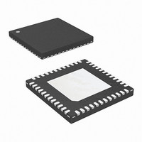
ISL6262CRZ Intersil, ISL6262CRZ Datasheet - Page 23

ISL6262CRZ
Manufacturer Part Number
ISL6262CRZ
Description
IC CORE REG 2PHASE 48-QFN
Manufacturer
Intersil
Datasheet
1.ISL6262CRZ.pdf
(27 pages)
Specifications of ISL6262CRZ
Applications
Converter, Intel IMVP-6
Voltage - Input
5 ~ 25 V
Number Of Outputs
1
Voltage - Output
0.3 ~ 1.5 V
Operating Temperature
-10°C ~ 100°C
Mounting Type
Surface Mount
Package / Case
48-VQFN
Lead Free Status / RoHS Status
Lead free / RoHS Compliant
Available stocks
Company
Part Number
Manufacturer
Quantity
Price
Company:
Part Number:
ISL6262CRZ
Manufacturer:
AMD
Quantity:
144
Part Number:
ISL6262CRZ
Manufacturer:
INTERSIL
Quantity:
20 000
Therefore, the output of the droop amplifier divided by the
total load current can be expressed as follows.
where R
the temperature coefficient of the copper. To achieve the
droop value independent from the temperature of the
inductor, it is equivalently expressed by the following.
The non-inverting droop amplifier circuit has the gain
K
G
Therefore, the temperature characteristics of gain of Vn is
described by:
For the G
Rseries = 2610kΩ, and Rpar = 11kΩ, RS
generates a desired G1, close to the feature specified in
Equation 20. The actual G1 at 25°C is 0.763. For different
G1 and NTC thermistor preference, the design file to
generate the proper value of Rntc, Rseries, Rpar, and
RS
Then, the individual resistors from each phase to the VSUM
node, labeled RS1 and RS2 in Figure 31, are then given by
the following equation.
So, Rs = 3650Ω. Once we know the attenuation of the RS
and RN network, we can then determine the droop amplifier
gain required to achieve the load line. Setting Rdrp1 =
1k_1%, then Rdrp2 is can be found using equation
Droop Impedance (Rdroop) = 0.0021 (V/A) as per the Intel
IMVP-6 specification, DCR = 0.0008Ω typical for a 0.36µH
inductor, Rdrp1 = 1kΩ and the attenuation gain (G1) = 0.77,
Rdrp2 is then given by
G
DCR T ( )
R
G
k
G
Rs
Rdrp2
Rdrp2
droopamp
droopamp
droop
1target
1
1
1
T ( )
T ( )
T ( )
EQV
=
2 RS
•
=
=
=
•
Δ
=
=
(
is provided by Intersil.
droop
1
is the desired gain of Vn over I
=
------------------------------------------------------ -
(
⎛
⎝
⎛
⎝
1target
G
1
+
----------------------------------------------- 1
DCR G1 25°C
-------------------------------------- - 1
0.0008 0.763
------------------------------------------ -
R
DCR
expressed as:
=
1
+
0.00393*(T-25)
EQV
n
2 R
T ( )
0.00393*(T-25)
T ( )
1
2 R
•
is the realized load line slope and 0.00393 is
G
+
R
•
•
25°C
•
1t
= 0.76, the Rntc = 10kΩ with b = 4300,
+
R
--------------- -
R
n
droop
•
DCR
-------------------
T ( )
arg
drp2
drp1
RS
droop
(
2
•
et
EQV
(
25
1
–
+
•
)
)
0.00393*(T-25)
(
⎞
⎠
≅
)
1
–
•
G
+
23
⎞
⎠
1kΩ
1t
0.00393*(T-25)
•
arg
R
drp1
≈
et
5.82kΩ
OUT
)
EQV
) k
• DCR/2.
•
= 1825Ω
droopamp
(EQ. 16)
(EQ. 17)
(EQ. 18)
(EQ. 19)
(EQ. 20)
(EQ. 21)
(EQ. 22)
ISL6262
Note, we choose to ignore the RO resistors because they do
not add significant error.
These designed values in Rn network are very sensitive to
layout and coupling factor of the NTC to the inductor. As only
one NTC is required in this application, this NTC should be
placed as close to the Channel 1 inductor as possible and
PCB traces sensing the inductor voltage should be go
directly to the inductor pads.
Once the board has been laid out, some adjustments may
be required to adjust the full load droop voltage. This is fairly
easy and can be accomplished by allowing the system to
achieve thermal equilibrium at full load, and then adjusting
Rdrp2 to obtain the appropriate load line slope.
To see whether the NTC has compensated the temperature
change of the DCR, the user can apply full load current and
wait for the thermal steady state and see how much the
output voltage will deviate from the initial voltage reading. A
good compensation can limit the drift to 2mV. If the output
voltage is decreasing with temperature increase, that ratio
between the NTC thermistor value and the rest of the
resistor divider network has to be increased. The user
should follow the evaluation board value and layout of NTC
as much as possible to minimize engineering time.
The 2.1mV/A load line should be adjusted by Rdrp2 based
on maximum current, not based on small current steps like
10A, as the droop gain might vary between each 10A steps.
Basically, if the max current is 40A, the required droop
voltage is 84mV. The user should have 40A load current on
and look for 84mV droop. If the drop voltage is less than
84mV, for example, 80mV. The new value will be calculated
by:
For the best accuracy, the effective resistance on the DFB
and VSUM pins should be identical so that the bias current
of the droop amplifier does not cause an offset voltage. In
the example above, the resistance on the DFB pin is Rdrp1
in parallel with Rdrop2, that is, 1K in parallel with 5.82K or
853Ω. The resistance on the VSUM pin is Rn in parallel with
RS
mismatch in the effective resistances is 1392 - 853 = 539Ω.
Do not let the mismatch get larger than 600Ω. To reduce the
mismatch, multiply both Rdrp1 and Rdrp2 by the appropriate
factor. The appropriate factor in the example is
1392/853 = 1.632. In summary, the predicted load line with
the designed droop network parameters based on the
Intersil design tool is shown in Figure 35.
Rdrp2_new
EQV
or 5.87K in parallel with 1.825K or 1392Ω. The
=
84mV
--------------- - Rdrp1
80mV
(
+
Rdrp2
) Rdrp1
–
May 15, 2006
FN9199.2


