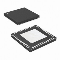
ISL6262CRZ Intersil, ISL6262CRZ Datasheet - Page 7

ISL6262CRZ
Manufacturer Part Number
ISL6262CRZ
Description
IC CORE REG 2PHASE 48-QFN
Manufacturer
Intersil
Datasheet
1.ISL6262CRZ.pdf
(27 pages)
Specifications of ISL6262CRZ
Applications
Converter, Intel IMVP-6
Voltage - Input
5 ~ 25 V
Number Of Outputs
1
Voltage - Output
0.3 ~ 1.5 V
Operating Temperature
-10°C ~ 100°C
Mounting Type
Surface Mount
Package / Case
48-VQFN
Lead Free Status / RoHS Status
Lead free / RoHS Compliant
Available stocks
Company
Part Number
Manufacturer
Quantity
Price
Company:
Part Number:
ISL6262CRZ
Manufacturer:
AMD
Quantity:
144
Part Number:
ISL6262CRZ
Manufacturer:
INTERSIL
Quantity:
20 000
SOFT - A capacitor from this pin to GND pin sets the
maximum slew rate of the output voltage. The SOFT pin is
the non-inverting input of the error amplifier.
OCSET - Overcurrent set input. A resistor from this pin to
VO sets DROOP voltage limit for OC trip. A 10µA current
source is connected internally to this pin.
VW - A resistor from this pin to COMP programs the
switching frequency (exa. 4.42kΩ ≅ 300kHz).
COMP - This pin is the output of the error amplifier.
FB - This pin is the inverting input of error amplifier.
FB2 - There is a switch between FB2 pin and the FB pin.
The switch is closed in single-phase operation and is
opened in two phase operation. The components connecting
to FB2 is to adjust the compensation in single phase
operation to achieve optimum performance.
VDIFF - This pin is the output of the differential amplifier.
VSEN - Remote core voltage sense input.
RTN - Remote core voltage sense return.
DROOP - Output of the droop amplifier. The voltage level on
this pin is the sum of Vo and the programmed droop voltage
by the external resistors.
DFB - Inverting input to droop amplifier.
VO - An input to the IC that reports the local output voltage.
VSUM - This pin is connected to the summation junction of
channel current sensing.
VIN - Battery supply voltage. It is used for input voltage
feedforward to improve the input line transient performance.
VSS - Signal ground. Connect to local controller ground.
VDD - 5V control power supply.
ISEN2 - Individual current sharing sensing for channel 2.
ISEN1 - Individual current sharing sensing for channel 1.
N/C - Not connected. Grounding this pin to signal ground in
the practical layout.
BOOT2 - This pin is the upper gate driver supply voltage for
phase 2. An internal boot strap diode is connected to the
PVCC pin.
UGATE2 - Upper MOSFET gate signal for phase 2.
PHASE2 - The phase node of phase 2. This pin should
connect to the source of upper MOSFET.
PGND2 - The return path of the lower gate driver for
phase 2.
LGATE2 - Lower-side MOSFET gate signal for phase 2.
PVCC - 5V power supply for gate drivers.
7
ISL6262
LGATE1 - Lower-side MOSFET gate signal for phase 1.
PGND1 - The return path of the lower gate driver for
phase 1.
PHASE1 - The phase node of phase 1. This pin should
connect to the source of upper MOSFET.
UGATE1 - Upper MOSFET gate signal for phase 1.
BOOT1 - This pin is the upper gate driver supply voltage for
phase 1. An internal boot strap diode is connected to the
PVCC pin.
VID0, VID1, VID2, VID3, VID4, VID5, VID6 - VID input with
VID0 is the least significant bit (LSB) and VID6 is the most
significant bit (MSB).
VR_ON - Digital input enable. A high level logic signal on
this pin enables the regulator.
DPRSLPVR - Deeper sleep enable signal. A high level logic
indicates the micro-processor is in Deeper Sleep Mode and
also indicates a slow C4 entry or exit rate with 41µA
discharging or charging the SOFT cap.
DPRSTP# - Deeper sleep slow wake up signal. A low level
logic signal on this pin indicates the micro-processor is in
deeper sleep mode.
CLK_EN# - Digital output for system PLL clock. Goes active
10µs after PGD_IN is active and Vcore is within 10% of Boot
voltage.
3V3 - 3.3V supply voltage for CLK_EN#.
May 15, 2006
FN9199.2


