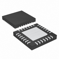
MAX8632ETI+T Maxim Integrated Products, MAX8632ETI+T Datasheet - Page 10

MAX8632ETI+T
Manufacturer Part Number
MAX8632ETI+T
Description
IC PWR SUPPLY DDR 28-TQFN
Manufacturer
Maxim Integrated Products
Datasheet
1.MAX8632ETIT.pdf
(29 pages)
Specifications of MAX8632ETI+T
Applications
Controller, DDR
Voltage - Input
2 ~ 28 V
Number Of Outputs
1
Voltage - Output
1.8V, 2.5V, 0.7 ~ 5.5 V
Operating Temperature
-40°C ~ 85°C
Mounting Type
Surface Mount
Package / Case
28-TQFN Exposed Pad
Output Voltage
1.8 V, 2.5 V, 0.7 V to 5.5 V
Output Current
15 A
Input Voltage
2 V to 28 V
Mounting Style
SMD/SMT
Maximum Operating Temperature
+ 85 C
Minimum Operating Temperature
- 40 C
Lead Free Status / RoHS Status
Lead free / RoHS Compliant
Integrated DDR Power-Supply Solution for
Desktops, Notebooks, and Graphic Cards
10
PIN
11
12
13
14
15
16
17
18
19
20
21
22
23
24
25
26
27
28
—
______________________________________________________________________________________
PGND2
PGND1
NAME
REFIN
SHDN
AV
GND
SKIP
VTTI
OUT
V
VTT
BST
TP0
V
DH
FB
LX
DL
EP
DD
IN
DD
Power Ground for VTT and VTTR. Connect PGND2 externally to the underside of the exposed pad.
Termination Power-Supply Output. Connect VTT to VTTS to regulate to V
Power-Supply Input Voltage for VTT and VTTR. Normally connected to the output of the buck regulator
for DDR application.
External Reference Input. This is used to regulate the VTT and VTTR outputs to V
Feedback Input for Buck Output. Connect to AV
output. For an adjustable output (0.7V to 5.5V), connect FB to a resistive divider from the output
voltage. FB regulates to +0.7V.
Output-Voltage Sense Connection. Connect to the positive terminal of the buck output filter capacitor.
OUT senses the output voltage to determine the on-time for the high-side switching MOSFET (Q1 in
Figure 8). OUT also serves as the buck output’s feedback input in fixed-output modes. When discharge
mode is enabled by OVP/UVP, the output capacitor is discharged through an internal 10Ω resistor
connected between OUT and GND. OUT also acts as the input to the VTT and VTTR UVLO detector.
Input-Voltage Sense Connection. Connect to input power source. V
time one-shot timer. IN voltage range is from 2V to 28V.
High-Side Gate-Driver Output. Swings from LX to BST. DH is low when in shutdown or UVLO.
External Inductor Connection. Connect LX to the input side of the inductor. LX is used for both current
limit and the return supply of the DH driver.
Boost Flying-Capacitor Connection. Connect to an external capacitor and diode according to Figure 8.
See the Boost-Supply Diode and Capacitor Selection (Buck) section.
Synchronous-Rectifier Gate-Driver Output. Swings from PGND to V
Supply Input for the DL Gate Drive. Connect to the +4.5V to +5.5V system supply voltage. Bypass to
PGND1 with a 1µF (min) ceramic capacitor.
Power Ground for Buck Controller. Connect PGND1 externally to the low-side FET’s source.
Analog Ground for Both Buck and LDO. Connect GND externally to the underside of the exposed pad.
Pulse-Skipping Control Input. Connect to AV
enable pulse-skipping operation.
Analog Supply Input for Both Buck and LDO. Connect to the +4.5V to +5.5V system supply voltage
with a series 10Ω resistor. Bypass to GND with a 1µF or greater ceramic capacitor.
Shutdown Control Input. Use to control buck output. A rising edge on SHDN clears the overvoltage-
and undervoltage-protection fault latches (see Tables 2 and 3). Connect to AV
This is a test pin. Must connect to GND externally.
Exposed pad. The exposed pad must be star-connected to GND and PGND2. See Special Layout
Considerations for LDO Section for more details.
DD
FUNCTION
for low-noise, forced-PWM mode. Connect to GND to
DD
for a +1.8V fixed output or to GND for a +2.5V fixed
Pin Description (continued)
DD
IN
.
is used only to set the PWM’s on-
REFIN
/ 2.
DD
REFIN
for normal operation.
/ 2.


