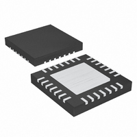
MAX8632ETI+T Maxim Integrated Products, MAX8632ETI+T Datasheet - Page 22

MAX8632ETI+T
Manufacturer Part Number
MAX8632ETI+T
Description
IC PWR SUPPLY DDR 28-TQFN
Manufacturer
Maxim Integrated Products
Datasheet
1.MAX8632ETIT.pdf
(29 pages)
Specifications of MAX8632ETI+T
Applications
Controller, DDR
Voltage - Input
2 ~ 28 V
Number Of Outputs
1
Voltage - Output
1.8V, 2.5V, 0.7 ~ 5.5 V
Operating Temperature
-40°C ~ 85°C
Mounting Type
Surface Mount
Package / Case
28-TQFN Exposed Pad
Output Voltage
1.8 V, 2.5 V, 0.7 V to 5.5 V
Output Current
15 A
Input Voltage
2 V to 28 V
Mounting Style
SMD/SMT
Maximum Operating Temperature
+ 85 C
Minimum Operating Temperature
- 40 C
Lead Free Status / RoHS Status
Lead free / RoHS Compliant
where V
allow about 20% more for additional losses because of
MOSFET output capacitances and low-side MOSFET
body-diode reverse-recovery charge dissipated in the
high-side MOSFET that is not well defined in the
MOSFET data sheet. Refer to the MOSFET data sheet
for thermal-resistance specifications to calculate the PC
board area needed to maintain the desired maximum
operating junction temperature with the above-calculat-
ed power dissipations. To reduce EMI caused by
switching noise, add a 0.1µF ceramic capacitor from the
high-side switch drain to the low-side switch source, or
add resistors in series with DH and DL to slow down the
switching transitions. Adding series resistors increases
the power dissipation of the MOSFET, so ensure that
this does not overheat the MOSFET.
Fast switching transitions cause ringing because of a
resonating circuit formed by the parasitic inductance
and capacitance at the switching nodes. This high-fre-
quency ringing occurs at LX’s rising and falling transi-
tions and can interfere with circuit performance and
generate EMI. To dampen this ringing, an optional
series RC snubber circuit is added across each switch.
Below is a simple procedure for selecting the value of
the series RC of the snubber circuit:
1) Connect a scope probe to measure V
2) Estimate the circuit parasitic capacitance (C
3) Estimate the circuit parasitic inductance (L
4) Calculate the resistor for critical dampening (R
5) The capacitor (C
Integrated DDR Power-Supply Solution for
Desktops, Notebooks, and Graphic Cards
22
and observe the ringing frequency, f
LX by first finding a capacitor value, which, when
connected from LX to PGND1, reduces the ringing
frequency by half. C
1/3rd the value of the capacitor value found.
the equation:
from the equation: R
the resistor value up or down to tailor the desired
damping and the peak voltage excursion.
times the value of C
______________________________________________________________________________________
GS
= V
L
PAR
MOSFET Snubber Circuit (Buck)
DD
= 5V. In addition to the losses above,
=
SNUB
(
2
PAR
π
PAR
SNUB
×
f
) should be at least 2 to 4
to be effective.
R
can then be calculated as
)
2
= 2π × f
1
×
C
PAR
R
R
.
x L
LX
PAR
to PGND1,
PAR
. Adjust
PAR
SNUB
) from
) at
)
The power loss of the snubber circuit (P
pated in the resistor and can be calculated as:
where V
frequency. Choose an R
the specific application’s derating rule for the power
dissipation calculated.
The current-sense method used in the MAX8632 makes
use of the on-resistance (R
MOSFET (Q2 in Figure 8). When calculating the current
limit, use the worst-case maximum value for R
the MOSFET data sheet, and add some margin for the
rise in R
to allow 0.5% additional resistance for each 1°C of tem-
perature rise.
The minimum current-limit threshold must be great
enough to support the maximum load current when the
current limit is at the minimum tolerance value. The val-
ley of the inductor current occurs at I
half the ripple current; therefore:
where I
threshold voltage divided by the on-resistance of Q2
(R
to AV
threshold is precisely 1/10th* the voltage seen at ILIM.
For an adjustable threshold, connect a resistive divider
from REF to GND with ILIM connected to the center tap.
The external 250mV to 2V adjustment range corresponds
to a 25mV to 200mV valley current-limit threshold. When
adjusting the current limit, use 1% tolerance resistors and
a divider current of approximately 10µA to prevent signifi-
cant inaccuracy in the valley current-limit tolerance.
Alternately, foldback current limit can be implemented
if the UVP latch option is not available. Foldback cur-
rent limit reduces the power dissipation of external
components so they can withstand indefinite overload
and short circuit, with automatic recovery after the over-
load or short circuit is removed. To implement foldback
current limit, connect a resistor from V
in Figures 7 and 8), in addition to the resistor-divider
*In the negative direction, the adjustable current limit is typically
-1/8th the voltage seen at ILIM.
DS(ON)Q2
I
LIM VAL
DD
LIM(VAL)
DS(ON)
IN
(
. In adjustable mode, the valley current-limit
P
is the input voltage and f
). For the 50mV default setting, connect ILIM
RSNUB
)
>
Setting the Current Limit (Buck)
with temperature. A good general rule is
I
equals the minimum valley current-limit
LOAD MAX
=
C
(
SNUB
SNUB
)
-
DS(ON)
×
Foldback Current Limit
power rating that meets
I
LOAD MAX
V
IN
2
SW
) of the low-side
(
LOAD(MAX)
×
OUT
RSNUB
is the switching
2
f
SW
)
×
DS(ON)
to ILIM (R6
LIR
) is dissi-
minus
from


