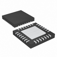
MAX8632ETI+T Maxim Integrated Products, MAX8632ETI+T Datasheet - Page 26

MAX8632ETI+T
Manufacturer Part Number
MAX8632ETI+T
Description
IC PWR SUPPLY DDR 28-TQFN
Manufacturer
Maxim Integrated Products
Datasheet
1.MAX8632ETIT.pdf
(29 pages)
Specifications of MAX8632ETI+T
Applications
Controller, DDR
Voltage - Input
2 ~ 28 V
Number Of Outputs
1
Voltage - Output
1.8V, 2.5V, 0.7 ~ 5.5 V
Operating Temperature
-40°C ~ 85°C
Mounting Type
Surface Mount
Package / Case
28-TQFN Exposed Pad
Output Voltage
1.8 V, 2.5 V, 0.7 V to 5.5 V
Output Current
15 A
Input Voltage
2 V to 28 V
Mounting Style
SMD/SMT
Maximum Operating Temperature
+ 85 C
Minimum Operating Temperature
- 40 C
Lead Free Status / RoHS Status
Lead free / RoHS Compliant
Integrated DDR Power-Supply Solution for
Desktops, Notebooks, and Graphic Cards
• The LX and PGND1 connections to the low-side
• When trade-offs in trace lengths must be made, it is
• Route high-speed switching nodes (BST, LX, DH,
• Input ceramic capacitors must be placed as close
Figure 9. Voltage-Positioned Output
26
thick copper PC boards (2oz vs. 1oz) can enhance
full-load efficiency by 1% or more. Correctly routing
PC board traces is a difficult task that must be
approached in terms of fractions of centimeters,
where a single mΩ of excess trace resistance caus-
es a measurable efficiency penalty.
MOSFET for current sensing must be made using
Kelvin-sense connections.
preferable to allow the inductor-charging path to be
made longer than the discharge path. For example,
it is better to allow some extra distance between the
input capacitors and the high-side MOSFET than to
allow distance between the inductor and the low-
side MOSFET or between the inductor and the out-
put filter capacitor.
and DL) away from sensitive analog areas (REF, FB,
and ILIM).
as possible to the high-side MOSFET drain and the
low-side MOSFET source. Position the MOSFETs so
the impedance between the input capacitor termi-
nals and the MOSFETs is as low as possible.
______________________________________________________________________________________
AV
FB
DD
MAX8632
PGND1
GND
OUT
V
BST
DH
DL
DD
LX
IN
The capacitor (or capacitors) at VTT should be placed
as close to VTT and PGND2 (pins 12 and 11) as possi-
ble to minimize the series resistance/inductance of the
trace. The PGND2 side of the capacitor must be short
with a low-impedance path to the exposed pad under-
neath the IC. The exposed pad must be star-connected
to GND (pin 24) and PGND2 (pin 11). Connect PGND1
(pin 23) separately to the nearby PGND plane at the
source of the low-side MOSFET. Do not connect this
pin directly to the exposed pad as this can inject unde-
sirable switching noise into the clean analog GND.
Instead, PGND1 (pin 23) is connected to PGND2 (pin
11) by the large PGND plane. A narrower trace can be
used to connect the output voltage on the VTT side of
the capacitor back to VTTS (pin 9). For best perfor-
mance, the VTTI bypass capacitor must be placed as
close to VTTI (pin 13) as possible. REFIN (pin 14)
should be separately routed with a clean trace and
adequately bypassed to GND. Refer to the MAX8632
evaluation kit data sheet for PC board guidelines.
Special Layout Considerations for LDO Section
+5V BIAS
SUPPLY
V
IN
R
POS
POSITIONED
VOLTAGE-
OUTPUT


