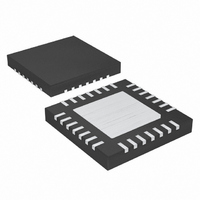
MAX8632ETI+T Maxim Integrated Products, MAX8632ETI+T Datasheet - Page 14

MAX8632ETI+T
Manufacturer Part Number
MAX8632ETI+T
Description
IC PWR SUPPLY DDR 28-TQFN
Manufacturer
Maxim Integrated Products
Datasheet
1.MAX8632ETIT.pdf
(29 pages)
Specifications of MAX8632ETI+T
Applications
Controller, DDR
Voltage - Input
2 ~ 28 V
Number Of Outputs
1
Voltage - Output
1.8V, 2.5V, 0.7 ~ 5.5 V
Operating Temperature
-40°C ~ 85°C
Mounting Type
Surface Mount
Package / Case
28-TQFN Exposed Pad
Output Voltage
1.8 V, 2.5 V, 0.7 V to 5.5 V
Output Current
15 A
Input Voltage
2 V to 28 V
Mounting Style
SMD/SMT
Maximum Operating Temperature
+ 85 C
Minimum Operating Temperature
- 40 C
Lead Free Status / RoHS Status
Lead free / RoHS Compliant
remains fixed) and less output voltage ripple. Penalties
for using higher inductor values include larger physical
size and degraded load-transient response, especially
at low input-voltage levels.
DC output accuracy specifications refer to the threshold
of the error comparator. When the inductor is in continu-
ous conduction, the MAX8632 regulates the valley of the
output ripple, so the actual DC output voltage is higher
than the trip level by 50% of the output ripple voltage. In
discontinuous conduction (SKIP = GND and I
I
level higher than the error-comparator threshold by
approximately 1.5% due to slope compensation.
The low-noise forced-PWM mode (SKIP = AV
ables the zero-crossing comparator, which controls the
low-side switch on-time. This forces the low-side gate-
drive waveform to constantly be the complement of the
high-side gate-drive waveform, so the inductor current
reverses at light loads while DH maintains a duty factor
of V
frequency fairly constant. However, forced-PWM opera-
tion comes at a cost where the no-load V
rent remains between 2mA and 20mA due to the
external MOSFET’s gate charge and switching frequen-
cy. Forced-PWM mode is most useful for reducing
audio frequency noise, improving load-transient
response, and providing sink-current capability for
dynamic output-voltage adjustment.
The current-limit circuit for the buck regulator portion of
the MAX8632 employs a unique “valley” current-sensing
algorithm that senses the voltage drop across LX and
PGND1 and uses the on-resistance of the rectifying
MOSFET (Q2 in Figure 8) as the current-sensing ele-
ment. If the magnitude of the current-sense signal is
above the valley current-limit threshold, the PWM con-
troller is not allowed to initiate a new cycle (Figure 4).
With valley current-limit sensing, the actual peak current
is greater than the valley current-limit threshold by an
amount equal to the inductor current ripple. Therefore,
the exact current-limit characteristic and maximum load
capability are a function of the current-sense resistance,
inductor value, and input voltage. When combined with
the undervoltage-protection circuit, this current-limit
method is effective in almost every circumstance.
Integrated DDR Power-Supply Solution for
Desktops, Notebooks, and Graphic Cards
14
LOAD(SKIP)
OUT
______________________________________________________________________________________
/ V
Current-Limit Buck Regulator (ILIM)
IN
), the output voltage has a DC regulation
Forced-PWM Mode ( SKIP = AV
. Forced-PWM mode keeps the switching
Valley Current Limit
DD
bias cur-
DD
LOAD
) dis-
DD
<
)
In forced-PWM mode, the MAX8632 also implements a
negative current limit to prevent excessive reverse induc-
tor currents when the buck regulator output is sinking
current. The negative current-limit threshold is set to
approximately 120% of the positive current limit and
tracks the positive current limit when V
The current-limit threshold is adjusted with an external
resistor-divider at ILIM. A 2µA to 20µA divider current is
recommended for accuracy and noise immunity.
The current-limit threshold adjustment range is from
25mV to 200mV. In the adjustable mode, the current-
limit threshold voltage (from PGND1 to LX) is precisely
1/10th the voltage seen at ILIM. The threshold defaults
to 50mV when ILIM is connected to AV
threshold for switchover to the 50mV default value is
approximately AV
Carefully observe the PC board layout guidelines to
ensure that noise and DC errors do not corrupt the differ-
ential current-sense signals seen between LX and GND.
Internal power-on reset (POR) occurs when AV
above approximately 2V, resetting the fault latch and
the soft-start counter, powering up the reference, and
preparing the buck regulator for operation. Until AV
reaches 4.25V (typ), AV
(UVLO) circuitry inhibits switching. The controller
inhibits switching by pulling DH low and holding DL low
Figure 2. Pulse-Skipping/Discontinuous Crossover Point
0
∆I
∆t
ON-TIME
=
V
IN
- V
L
OUT
DD
- 1V.
POR, UVLO, and Soft-Start
TIME
DD
undervoltage-lockout
ILIM
DD
I
I
PEAK
LOAD
is adjusted.
. The logic
= I
DD
PEAK
/ 2
rises
DD


