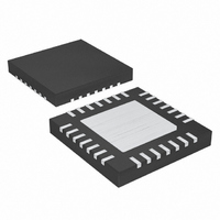
MAX8632ETI+T Maxim Integrated Products, MAX8632ETI+T Datasheet - Page 20

MAX8632ETI+T
Manufacturer Part Number
MAX8632ETI+T
Description
IC PWR SUPPLY DDR 28-TQFN
Manufacturer
Maxim Integrated Products
Datasheet
1.MAX8632ETIT.pdf
(29 pages)
Specifications of MAX8632ETI+T
Applications
Controller, DDR
Voltage - Input
2 ~ 28 V
Number Of Outputs
1
Voltage - Output
1.8V, 2.5V, 0.7 ~ 5.5 V
Operating Temperature
-40°C ~ 85°C
Mounting Type
Surface Mount
Package / Case
28-TQFN Exposed Pad
Output Voltage
1.8 V, 2.5 V, 0.7 V to 5.5 V
Output Current
15 A
Input Voltage
2 V to 28 V
Mounting Style
SMD/SMT
Maximum Operating Temperature
+ 85 C
Minimum Operating Temperature
- 40 C
Lead Free Status / RoHS Status
Lead free / RoHS Compliant
For Quick-PWM controllers, stability is determined by
the value of the ESR zero relative to the switching fre-
quency. The boundary of instability is given by the fol-
lowing equation:
If C
in Figure 8, the f
gle capacitor.
For a typical 600kHz application, the ESR zero frequen-
cy must be well below 190kHz, preferably below
100kHz. Two 150µF/4V Sanyo POS capacitors are used
to provide 12mΩ (max) of R
42kHz, well within the bounds of stability.
Do not put high-value ceramic capacitors directly
across the feedback sense point without taking precau-
tions to ensure stability. Large ceramic capacitors can
have a high-ESR zero frequency and cause erratic,
unstable operation. However, it is easy to add enough
series resistance by placing the capacitors a couple of
inches downstream from the feedback sense point,
which should be as close as possible to the inductor.
Unstable operation manifests itself in two related but
distinctly different ways: double pulsing and fast-feed-
back loop instability. Double pulsing occurs due to
noise on the output or because the ESR is so low that
there is not enough voltage ramp in the output voltage
signal. This “fools” the error comparator into triggering
a new cycle immediately after the 400ns minimum off-
time period has expired.
Double pulsing is more annoying than harmful, result-
ing in nothing worse than increased output ripple.
However, it can indicate the possible presence of loop
instability due to insufficient ESR. Loop instability can
result in oscillations at the output after line or load
steps. Such perturbations are usually damped but can
cause the output voltage to rise above or fall below the
tolerance limits. The easiest method for checking stabil-
ity is to apply a very fast zero-to-max load transient and
carefully observe the output-voltage-ripple envelope for
overshoot and ringing. It can help to simultaneously
monitor the inductor current with an AC current probe.
Do not allow more than one cycle of ringing after the
initial step-response under/overshoot.
Integrated DDR Power-Supply Solution for
Desktops, Notebooks, and Graphic Cards
20
where
OUT
______________________________________________________________________________________
:
consists of multiple same-value capacitors, as
ESR
f
ESR
remains the same as that of a sin-
=
f
ESR
2
ESR
π
×
≤
Stability Requirements
. This results in a zero at
R
f
ESR
SW
π
1
×
C
OUT
A minimum value of 20µF is needed to stabilize the VTT
output. This value of capacitance limits the regulator’s
unity-gain bandwidth frequency to approximately 1.8MHz
(typ) to allow adequate phase margin for stability. To
keep the capacitor acting as a capacitor within the regu-
lator’s bandwidth, it is important that ceramic caps with
low ESR and ESL be used.
Since the gain bandwidth is also determined by the
transconductance of the output FETs, which increases
with load current, the output capacitor may need to be
greater than 20µF if the load current exceeds 1.5A, but
can be smaller than 20µF if the maximum load current
is less than 1.5A. As a guideline, choose the minimum
capacitance and maximum ESR for the output capaci-
tor using the following:
R
frequency given by approximately:
Once these conditions for stability are met, additional
capacitors, including those of electrolytic and tantalum
types, can be connected in parallel to the ceramic
capacitor (if desired) to further suppress noise or volt-
age ripple at the output.
The VTTR buffer is a scaled-down version of the VTT
regulator, with much smaller output transconductance.
Its compensation cap can therefore be smaller, and its
ESR larger, than what is required for its larger counter-
part. For typical applications requiring load current up
to ±15mA, a ceramic cap with a minimum value of 1µF
is recommended (R
between VTTR and the analog ground plane.
Both the VTT and VTTR output stages are powered
from the same VTTI input. Their output voltages are ref-
erenced to the same REFIN input. The value of the VTTI
bypass capacitor is chosen to limit the amount of rip-
ple/noise at VTTI, or the amount of voltage dip during a
load transient. Typically VTTI is connected to the output
of the buck regulator, which already has a large bulk
ESR
VTTR Output Capacitor Selection (LDO)
VTT Output Capacitor Selection (LDO)
value is measured at the unity-gain-bandwidth
VTTI Input Capacitor Selection (LDO)
C
R
ESR MAX
OUT MIN
f
GBW
_
_
ESR
=
=
=
C
20
5
OUT
< 0.3Ω). Connect this cap
36
m
µ
Ω
F
×
×
×
I
I
LOAD
I
LOAD
1 5
1 5
LOAD
1 5
.
.
.
A
A
A


