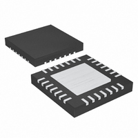
MAX8632ETI+T Maxim Integrated Products, MAX8632ETI+T Datasheet - Page 25

MAX8632ETI+T
Manufacturer Part Number
MAX8632ETI+T
Description
IC PWR SUPPLY DDR 28-TQFN
Manufacturer
Maxim Integrated Products
Datasheet
1.MAX8632ETIT.pdf
(29 pages)
Specifications of MAX8632ETI+T
Applications
Controller, DDR
Voltage - Input
2 ~ 28 V
Number Of Outputs
1
Voltage - Output
1.8V, 2.5V, 0.7 ~ 5.5 V
Operating Temperature
-40°C ~ 85°C
Mounting Type
Surface Mount
Package / Case
28-TQFN Exposed Pad
Output Voltage
1.8 V, 2.5 V, 0.7 V to 5.5 V
Output Current
15 A
Input Voltage
2 V to 28 V
Mounting Style
SMD/SMT
Maximum Operating Temperature
+ 85 C
Minimum Operating Temperature
- 40 C
Lead Free Status / RoHS Status
Lead free / RoHS Compliant
The overshoot during a full-load to no-load transient
due to stored inductor energy can be calculated as:
The output-voltage adjustable range for continuous-
conduction operation is restricted by the nonadjustable
minimum off-time one-shot. For best dropout perfor-
mance, use the slower (200kHz) on-time setting. When
working with low input voltages, the duty-factor limit
must be calculated using worst-case values for on- and
off-times. Manufacturing tolerances and internal propa-
gation delays introduce an error to the TON K-factor.
This error is greater at higher frequencies (see Table
1). Also, keep in mind that transient-response perfor-
mance of buck regulators operated too close to
dropout is poor, and bulk output capacitance must
often be added (see the V
Procedure section).
The absolute point of dropout is when the inductor cur-
rent ramps down during the minimum off-time (∆I
as much as it ramps up during the on-time (∆I
ratio h = ∆I
to slew the inductor current higher in response to
increased load, and must always be greater than 1. As
h approaches 1, the absolute minimum dropout point,
the inductor current cannot increase as much during
each switching cycle, and V
unless additional output capacitance is used.
A reasonable minimum value for h is 1.5, but adjusting
this up or down allows trade-offs between V
capacitance, and minimum operating voltage. For a
given value of h, the minimum operating voltage can be
calculated as:
where V
drops in the discharge and charge paths (see the On-
Time One-Shot (TON) section), t
Electrical Characteristics, and K is taken from Table 1.
The absolute minimum input voltage is calculated with
h = 1.
V
IN MIN
(
)
DROP1
=
UP
V
1 -
SOAR
Integrated DDR Power-Supply Solution for
/ ∆I
Applications Information
V
and V
Desktops, Notebooks, and Graphic Cards
OUT
h
DOWN
______________________________________________________________________________________
Dropout Performance (Buck)
=
×
+
DROP2
∆
t
2
OFF MIN
I
V
K
×
LOAD MAX
indicates the controller’s ability
DROP
C
(
SAG
OUT
(
are the parasitic voltage
1
)
SAG
equation in the Design
×
)
OFF(MIN)
2
+
V
greatly increases,
V
OUT
×
DROP
L
2
SAG
is from the
-
V
UP
, output
DROP
DOWN
). The
1
)
If the calculated V
minimum input voltage, then the operating frequency
must be reduced or output capacitance added to
obtain an acceptable V
anticipated, calculate V
transient response.
A dropout design example follows:
V
f
K = 1.7µs
t
V
h = 1.5
In applications where fast-load transients occur, the
output voltage changes instantly by R
∆I
put capacitors for such applications, and maximizes
the output-voltage AC and DC tolerance window in
tight-tolerance applications.
Figure 9 shows the connection of OUT and FB in a volt-
age-positioned circuit. In nonvoltage-positioned cir-
cuits, the MAX8632 regulates at the output capacitor. In
voltage-positioned circuits, the MAX8632 regulates on
the inductor side of the voltage-positioning resistor.
V
Careful PC board layout is critical to achieve low
switching losses and clean, stable operation. The
switching power stage requires particular attention. If
possible, mount all the power components on the top
side of the board, with their ground terminals flush
against one another. Follow these guidelines for good
PC board layout:
• Keep the high-current paths short, especially at the
• Keep the power traces and load connections short.
SW
OFF(MIN)
V
OUT
DROP1
OUT
LOAD
IN MIN
ground terminals. This practice is essential for sta-
ble, jitter-free operation.
This practice is essential for high efficiency. Using
V
(
= 600kHz
OUT VPS
= 2.5V
is reduced to:
. Voltage positioning allows the use of fewer out-
)
= V
(
= 450ns
=
DROP2
)
1
=
-
2 5
V
.
1 5
= 100mV
OUT NO LOAD
IN(MIN)
.
PC Board Layout Guidelines
V
Voltage Positioning (Buck)
1 7
×
+
.
(
SAG
450
0 1
µ
SAG
.
s
_
is greater than the required
V
. If operation near dropout is
ns
to be sure of adequate
)
+
-
0 1
R
.
POS
V
ESR
-
0 1
×
.
× C
V
I
LOAD
=
OUT
4 3
.
25
V
×


