ISL6225CA Intersil, ISL6225CA Datasheet

IC CTRLR DDR DRAM, SDRAM 28QSOP

ISL6225CA

Manufacturer Part Number
ISL6225CA
Description
IC CTRLR DDR DRAM, SDRAM 28QSOP
Manufacturer
Intersil
Datasheet

Specifications of ISL6225CA

Applications
Controller, DDR DRAM, SDRAM
Voltage - Input
5 ~ 24 V
Number Of Outputs
2
Voltage - Output
0.9 ~ 5.5 V
Operating Temperature
-10°C ~ 85°C
Mounting Type
Surface Mount
Package / Case
28-QSOP
Lead Free Status / RoHS Status
Contains lead / RoHS non-compliant

Available stocks

Company
Part Number
Manufacturer
Quantity
Price
Part Number:
ISL6225CA
Manufacturer:
INTERSIL
Quantity:
36
Part Number:
ISL6225CA
Manufacturer:
Intersil
Quantity:
467
Part Number:
ISL6225CA
Manufacturer:
ISL
Quantity:
20 000
Company:
Part Number:
ISL6225CA
Quantity:
292
Company:
Part Number:
ISL6225CA
Quantity:
292
Part Number:
ISL6225CA-T
Manufacturer:
INTERSIL
Quantity:
980
Part Number:
ISL6225CA-T
Manufacturer:
INTERSIL
Quantity:
20 000
Part Number:
ISL6225CAZ
Manufacturer:
Intersil
Quantity:
1 889
Part Number:
ISL6225CAZ
Manufacturer:
INTERSIL
Quantity:
20 000
Part Number:
ISL6225CAZ-T
Manufacturer:
INTERSIL
Quantity:
1 608
Part Number:
ISL6225CAZ-T
Manufacturer:
INTERSIL
Quantity:
20 000
Company:
Part Number:
ISL6225CAZ-T
Quantity:
1 500
Dual Mobile-Friendly PWM Controller with
DDR Memory Option
The ISL6225 dual PWM controller delivers high efficiency and
tight regulation from two voltage regulating synchronous buck
DC/DC converters. The ISL6225 PWM power supply controller
was designed especially for DDR DRAM, SDRAM, and graphic
chipset applications in high performance desknote PCs,
notebook PCs, sub-notebook PCs, and PDAs.
Automatic mode selection of constant-frequency synchronous
rectification at heavy load, and hysteretic diode-emulation at
light load, assure high efficiency over a wide range of
conditions. The hysteretic mode of operation can be disabled
separately on each PWM converter if constant-frequency
continuous-conduction operation is desired for all load levels.
Efficiency is further enhanced by using the lower MOSFET
r
Voltage-feed-forward ramp modulation, average current mode
control, and internal feedback compensation provide fast
response to input voltage and output load transients. Input
current ripple is minimized by channel to channel PWM
phase shift of 0°, 90°, or 180° determined by input voltage
and status of the DDR pin.
The ISL6225 can control two independent output voltages
adjustable from 0.9V to 5.5V or, by activating the DDR pin,
transform into a complete DDR memory power supply
solution. In DDR mode, CH2 output voltage VTT tracks CH1
output voltage VDDQ. CH2 output can both source and sink
current, an essential power supply feature for DDR memory
systems. The reference voltage VREF required by DDR
memory is generated as well.
In dual power supply applications the ISL6225 monitors the
output voltage of both CH1 and CH2. An independent
PGOOD (power good) signal is asserted for each channel
after the soft-start sequence has completed, and the output
voltage is within ±10% of the set point. In DDR mode CH1
generates the only PGOOD signal.
Built-in overvoltage protection prevents the output from
going above 115% of the set point by holding the lower
MOSFET on and the upper MOSFET off. When the output
voltage decays below the overvoltage threshold, normal
operation automatically resumes. Once the soft-start
sequence has completed, under-voltage protection may
latch the ISL6225 off if either output drops below 75% of its
set point value.
Adjustable overcurrent protection (OCP) monitors the
voltage drop across the r
more precise current-sensing is required, an external current
sense resistor may be used.
DS(ON)
as the current sense element.
DS(ON)
®
1
of the lower MOSFET. If
Data Sheet
1-888-INTERSIL or 321-724-7143
CAUTION: These devices are sensitive to electrostatic discharge; follow proper IC Handling Procedures.
Features
• Provides regulated output voltage in the range of 0.9V-5.5V
• Complete DDR memory power solution
• No current-sense resistor required
• Under-voltage lock-out on V
• Dual input voltage mode operation
• Excellent dynamic response
• Power-good signal for each channel
• 300kHz switching frequency
• Pb-Free Available (RoHS Compliant)
Applications
• Mobile PCs
• PDAs
• Hand-held portable instruments
Ordering Information
NOTES:
ISL6225CA
ISL6225CAZ (Note 1)
ISL6225CAZA (Note 1)
1. Intersil Pb-free products employ special Pb-free material sets; molding
2. Add “-T” for Tape and Reel.
December 28, 2004
- High efficiency over wide load range
- Synchronous buck converter with hysteretic operation at
- Inhibit Hysteretic mode on one, or both channels
- VTT tracks VDDQ/2
- VDDQ/2 buffered reference output
- Uses MOSFET r
- Optional current-sense resistor for precision overcurrent
- Operates directly from battery 5V to 24V input
- Operates from 3.3V or 5V system rail
- VCC from 5V only
- Combined voltage feed-forward and average current
- 180° channel to channel phase operation for reduced input
- 0° channel to channel phase operation in DDR mode for
- 90° channel to channel phase operation for reduced input
PART NUMBER
compounds/die attach materials and 100% matte tin plate termination
finish, which are RoHS compliant and compatible with both SnPb and
Pb-free soldering operations. Intersil Pb-free products are MSL
classified at Pb-free peak reflow temperatures that meet or exceed
the Pb-free requirements of IPC/JEDEC J STD-020.
light load
mode control
ripple when not in DDR mode
reduced channel interference
ripple in DDR mode when VIN is at GND.
All other trademarks mentioned are the property of their respective owners.
|
Intersil (and design) is a registered trademark of Intersil Americas Inc.
Copyright © Intersil Americas Inc. 2002-2004. All Rights Reserved
DS(ON)
TEMP. (°C)
-10 to 85
-10 to 85 28 Ld SSOP (Pb-free) M28.15
CC
pin
28 Ld SSOP
PACKAGE
ISL6225
FN9049.7
M28.15
DWG. #
PKG.

Related parts for ISL6225CA

ISL6225CA Summary of contents

Page 1

... TEMP. (°C) ISL6225CA - ISL6225CAZ (Note 1) - SSOP (Pb-free) M28.15 ISL6225CAZA (Note 1) - SSOP (Pb-free) M28.15 NOTES: 1. Intersil Pb-free products employ special Pb-free material sets; molding compounds/die attach materials and 100% matte tin plate termination finish, which are RoHS compliant and compatible with both SnPb and Pb-free soldering operations ...

Page 2

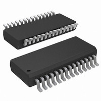
Pinout 2 ISL6225 ISL6225 SSOP-28 TOP VIEW 28 VCC GND 1 LGATE1 2 27 LGATE2 PGND1 3 26 PGND2 PHASE1 4 25 PHASE2 UGATE1 5 24 UGATE2 BOOT1 6 23 BOOT2 ISEN1 7 22 ISEN2 EN1 8 21 EN2 20 ...

Page 3

Absolute Maximum Ratings Bias Voltage ...

Page 4

Electrical Specifications Recommended Operating Conditions, Unless Otherwise Noted. (Continued) PARAMETER PWM CONVERTERS Load Regulation VSEN pin bias current V pin input impedance OUT Undervoltage Shut-Down Level Overvoltage Shut-Down GATE DRIVERS Upper Drive Pull-Up Resistance Upper Drive Pull-Down Resistance Lower Drive ...

Page 5

Functional Pin Description GND (Pin 1) Signal ground for the IC. LGATE1, LGATE2 (Pin 2, 27) These are outputs of the lower MOSFET drivers. PGND1, PGND2 (Pin 3, 26) These pins provide the return connection for lower gate drivers. These ...

Page 6

Generic Application Circuits ENABLE +V IN +3.3V TO +24V +5V FIGURE 1. ISL6225 APPLICATION CIRCUIT FOR TWO CHANNEL POWER SUPPLY ENABLE OCSET1 +V IN +3.3V TO +24V +5V PG2/VREF VREF +1.25V FIGURE 2. ISL6225 APPLICATION CIRCUIT FOR COMPLETE DDR MEMORY ...

Page 7

Block Diagram BOOT1 UGATE1 PHASE1 ADAPTIVE DEAD-TIME DIODE EMULATION PGND1 V/I SAMPLE TIMING PWM/HYS TRANSITION LGATE1 VCC + MODE CHANGE COMP 1 - SAME STATE FOR 8 CLOCK CYCLES REQUIRED TO CHANGE PWM OR HYS MODE HYSTERETIC COMPARATOR 1 - ...

Page 8

Description Operation The ISL6225 is a dual channel PWM controller intended for use in power supplies for graphic chipset, SDRAM, DDR DRAM or other low voltage power applications in modern notebook and sub-notebook PCs. The IC integrates two control circuits ...

Page 9

Automatic Operation Mode Control In nominal currents the synchronous buck converter operates in continuous-conduction constant-frequency mode. This mode of operation achieves higher efficiency due to the substantially lower voltage drop across the synchronous MOSFET compared to a Schottky diode. In ...

Page 10

The hysteretic comparator initiates the PWM signal when the output voltage gets below the lower threshold and terminates the PWM signal when the output voltage rises above the upper threshold. A spread or hysteresis between these two thresholds determines the ...

Page 11

The zero frequency, the amplifier high-frequency gain, and the modulator gain are chosen to satisfy most typical applications. The crossover frequency will appear at the point where the modulator attenuation equals the amplifier high frequency gain. The only task that ...

Page 12

If load step is strong enough to pull output voltage lower than the undervoltage threshold, the chip shuts down immediately. Because of the nature of the used current sensing technique, and to accommodate wide range of the r variation, the ...

Page 13

... Figure 15 depicts the DDR solution in the case where the 5V system rail is used as a primary voltage source. For detailed information on the circuit, including a Bill-of- Materials and circuit board description, see Application Note AN9995. Also see Intersil’s web site (http://www.intersil.com) for the latest information out-of-phase ...

Page 14

CR1 BAT54 WT1 + 0.15µF 1.0µF 10µ +2.50V 10µH 3.0A 1/2 FDS6912A 2.00K 17.8K 330µF C11 2/2 FDS6912A 15nF VPULLUP 100K 10K 100K POWER GOOD CH1 ENABLE POWER ...

Page 15

CR1 BAT54 WT1 + 0.15µF 1.0µF 10µ +2.50V 4.7µH 3.0A 1/2 FDS6912A 2.00K 17.8K 330µF C11 2/2 FDS6912A 15nF VPULLUP 10K 100K 100K POWER GOOD CH1 ENABLE POWER ...

Page 16

CR1 BAT54 WT1 + 0.15µF 1.0µF 10µ 10µH 1/2 FDS6912A 2.00K 6.65K 330µF C12 2/2 FDS6912A 15nF VPULLUP 100K 10K 100K POWER GOOD CH1 ENABLE POWER GOOD CH2 ...

Page 17

CR1 BAT54 WT1 + 1.0µF 0.15µF 10µ 4.6µH +2.50V ~ 6.0A 1/2 FDS6912A 3.0A VDDQ 17.8K 330µF C12 2/2 FDS6912A 15nF VPULLUP 10K 100K 100K POWER GOOD CH1 ...

Page 18

CR1 BAT54 WT1 + 1.0µF 10µF 0.15µ 4.6µH +2.50V 3.0A ~ 6.0A 1/2 FDS6912A VDDQ 17.8K 330µF C12 2/2 FDS6912A 15nF VPULLUP 100K 10K 100K POWER GOOD CH1 ...

Page 19

... Accordingly, the reader is cautioned to verify that data sheets are current before placing orders. Information furnished by Intersil is believed to be accurate and reliable. However, no responsibility is assumed by Intersil or its subsidiaries for its use; nor for any infringements of patents or other rights of third parties which may result from its use ...

Related keywords