ISL6563CR-T Intersil, ISL6563CR-T Datasheet
ISL6563CR-T
Specifications of ISL6563CR-T
Available stocks


Related parts for ISL6563CR-T


ISL6563CR-T Summary of contents
Page 1
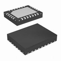
... RANGE (Note 2) MARKING (°C) ISL6563CRZ 65 63CRZ 4x4 QFN L24.4x4B ISL6563CRZ-T (Note 1) 65 63CRZ 4x4 QFN L24.4x4B ISL6563CRZ-TK (Note 1) 65 63CRZ 4x4 QFN L24.4x4B ISL6563IRZ 65 63IRZ - 4x4 QFN L24.4x4B ISL6563IRZ-T (Note 1) 65 63IRZ - 4x4 QFN L24.4x4B ISL6563EVAL1 ...
Page 2
Block Diagram OVP WHILE DISABLED 1.65V/1.95V + - OVP + 200mV - COMP VID0 VID1 VID2 TTL D/A CONVERTER VID3 (VID DAC) EA VID4 DACSEL/VID5 + VRM10 - FB Σ DROOP SOURCE OFFSET SOURCE GND OFS ENLL VCC SSEND POWER-ON ...
Page 3
Simplified Power System Diagram +5V IN 5-6 VID Typical Application +12V IN + VCC DACSEL/VID12 VID4 VID3 VID2 VID1 VID0 VRM10 R ISEN ISEN SSEND R’ OFS ISL6563 ENLL OFS R OFS COMP ...
Page 4
... QFN Package (Notes 3, 4 0.3V Maximum Junction Temperature . . . . . . . . . . . . . . . . . . . . . . +150°C BOOT - 0. 0.3V Maximum Storage Temperature Range . . . . . . . . . .-65°C to +150°C BOOT Pb-Free Reflow Profile .see link below http://www.intersil.com/pbfree/Pb-FreeReflow.asp = 5V 0°C to +85°C, Unless Otherwise Specified TEST CONDITIONS I ; ENLL = high VCC VCC Rising ...
Page 5
Electrical Specifications Test Conditions: V PARAMETER OVERCURRENT PROTECTION Overcurrent Trip Level PROTECTION Overvoltage Threshold while IC Disabled Overvoltage Threshold Overvoltage Hysteresis SWITCHING TIME UGATE Rise Time (Note 6) LGATE Rise Time (Note 6) UGATE Fall Time (Note 6) LGATE Fall ...
Page 6
Functional Pin Description VCC (Pin 8) Bias supply for the IC’s small-signal circuitry. Connect this pin supply and locally decouple using a quality 0.1µF ceramic capacitor. PVCC (Pin 16) Power supply pin for the MOSFET drives. Connect ...
Page 7
For more information, refer to the ‘Output Voltage Offset Programming’ paragraph. SSEND (Pin 10) This pin is an end of Soft-Start (SS) indicator; open drain output device stays ON during soft-start, and goes open when soft-start ends. Operation Figure 1 ...
Page 8
Internal average channel current is fed into the FB pin; the voltage thus developed across R is equal to the droop voltage. 1 Assuming identical power switch selection on the two channels, Equation 4 determines the current ...
Page 9
... In order to fully realize the thermal advantage important that each channel in a multiphase converter be controlled to deliver about the same current at any load level. Intersil multiphase controllers ensure current balance by comparing each channel’s current to the average current delivered by all channels and making appropriate adjustments to each channel’ ...
Page 10
TABLE 1. AMD HAMMER VOLTAGE IDENTIFICATION CODES (Continued) VID4 VID3 VID2 VID1 ...
Page 11
TABLE 3. VRM10 VOLTAGE IDENTIFICATION CODES VID4 VID3 VID2 VID1 VID0 ...
Page 12
In VRM10 setting, the ISL6563 checks for a change in the VID code six times each switching cycle new code is established and it stays the same for 3 consecutive readings, the ISL6563 recognizes the change and increments ...
Page 13
... This design guide is intended to provide a high-level explanation of the steps necessary to create a multiphase power converter assumed that the reader is familiar with many of the basic skills and techniques referenced below. In addition to this guide, Intersil provides complete reference designs that include schematics, bills of materials, and 13 ISL6563 example board layouts for all common microprocessor applications ...
Page 14
The above equation assumes the current through the lower MOSFET is always positive; if so, the total power dissipated in each lower MOSFET is approximated by the summation of P and P . LMOS1 LMOS2 UPPER MOSFET POWER CALCULATION In ...
Page 15
The feedback resistor has already been chosen as 1 outlined in “Load Line Regulation Resistor” on page 14. Select a target bandwidth for the compensated system, f The target bandwidth must be large enough to ensure adequate transient ...
Page 16
The output inductors must be capable of assuming the entire load current before the output voltage decreases more than ΔV . This places an upper limit on inductance. MAX ⋅ ⋅ OUT ≤ ⋅ ( ΔV ΔI ...
Page 17
High frequency decoupling capacitors should be placed as close to the power pins of the load, or for that reason, to any decoupling target they are meant for, as physically possible. Attention should be paid as not to add inductance ...
Page 18
... Accordingly, the reader is cautioned to verify that data sheets are current before placing orders. Information furnished by Intersil is believed to be accurate and reliable. However, no responsibility is assumed by Intersil or its subsidiaries for its use; nor for any infringements of patents or other rights of third parties which may result from its use ...
Page 19
Package Outline Drawing L24.4x4B 24 LEAD QUAD FLAT NO-LEAD PLASTIC PACKAGE Rev 3, 4/10 4.00 PIN 1 INDEX AREA (4X) 0.15 TOP VIEW ( TYP ) ( TYPICAL RECOMMENDED LAND PATTERN 19 ISL6563 ...