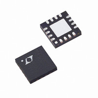
LT3582EUD-12#PBF Linear Technology, LT3582EUD-12#PBF Datasheet - Page 16

LT3582EUD-12#PBF
Manufacturer Part Number
LT3582EUD-12#PBF
Description
IC DC/DC CONV +/-12V 16-QFN
Manufacturer
Linear Technology
Type
Step-Up (Boost), Invertingr
Datasheet
1.LT3582EUDPBF.pdf
(28 pages)
Specifications of LT3582EUD-12#PBF
Internal Switch(s)
Yes
Synchronous Rectifier
No
Number Of Outputs
2
Voltage - Output
±12V
Current - Output
350mA, 600mA
Voltage - Input
2.55 ~ 5.5 V
Operating Temperature
-40°C ~ 125°C
Mounting Type
Surface Mount
Package / Case
16-WQFN Exposed Pad
Primary Input Voltage
3.6V
No. Of Outputs
2
Output Voltage
12V
Output Current
600mA
No. Of Pins
16
Operating Temperature Range
-40°C To +125°C
Msl
MSL 1 - Unlimited
Rohs Compliant
Yes
Lead Free Status / RoHS Status
Lead free / RoHS Compliant
Power - Output
-
Frequency - Switching
-
Available stocks
Company
Part Number
Manufacturer
Quantity
Price
LT3582/LT3582-5/LT3582-12
APPLICATIONS INFORMATION
tion voltage, the remaining output is activated and ramps
under control of its respective RAMP pin (see Figure 8).
The power-up sequencing concludes when both outputs
have reached regulation.
Evaluating PUSEQ Settings (LT3582 Only): After SHDN
rises, the LT3582 uses the PUSEQ confi guration found
in OTP . The effects of differing PUSEQ settings can be
observed without writing to OTP by taking the following
actions:
1. Write the SWOFF bit high, stopping both converters
2. Write the desired settings to the PUSEQ bits in REG2.
3. Set the RSEL2 bit high which selects the REG2 con-
4. Write SWOFF low which restarts both converters.
This will initiate the desired power-up sequence that can
be observed with an oscilloscope.
Power-Down Discharge (PDDIS bit)
The PDDIS bit is used to enable power-down discharge.
This bit is pre-confi gured to a “1” for the LT3582-5 and
LT3582-12, thus enabling power-down discharge.Setting
PDDIS = 0 disables the power-down discharge causing
the chip to shut down immediately after SHDN falls.
16
and discharging the RAMP pins.
fi guration settings.
0.5V/DIV
0.5V/DIV
V
V
V
V
5V/DIV
5V/DIV
RAMPN
RAMPP
Figure 8. Power-Up Sequencing (PUSEQ = 10)
VOUTP
VOUTN
RAMPP
5ms/DIV
RAMPN
The PDDIS bit must only be set in conjunction with
PUSEQ being set to 11. Driving SHDN low, with power-
down discharge enabled (PDDIS = 1) causes the chip to
power-down after fi rst discharging the output voltages.
Specifi cally, driving SHDN low causes the following se-
quence of events to happen:
1. Both converters are turned off.
2. Discharge currents are enabled to discharge the output
3. The chip waits until the output voltages have discharged
4. Discharge currents are disabled and the LT3582 powers
Since the LT3582 series won’t power-down until both
outputs are discharged (when power-down sequencing is
enabled), make sure V
This is not a problem in most topologies. However, read
the section Output Disconnect Operating Limits for ad-
ditional information.
capacitors
• See Electrical Characteristics for I
• See Electrical Characteristics for I
to within ~0.5V to ~1.5V of ground.
down.
I
helps discharge V
CAPP-PDS
3582512 F08
which help discharge V
OUTP
OUTN
and V
OUTN
OUTP
can be grounded.
VOUTN-PDS
VOUTP-PDS
and CAPP
3582512fb
which
and


