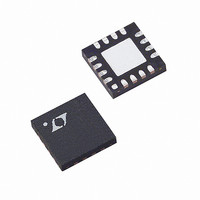
LT3582EUD-12#PBF Linear Technology, LT3582EUD-12#PBF Datasheet - Page 21

LT3582EUD-12#PBF
Manufacturer Part Number
LT3582EUD-12#PBF
Description
IC DC/DC CONV +/-12V 16-QFN
Manufacturer
Linear Technology
Type
Step-Up (Boost), Invertingr
Datasheet
1.LT3582EUDPBF.pdf
(28 pages)
Specifications of LT3582EUD-12#PBF
Internal Switch(s)
Yes
Synchronous Rectifier
No
Number Of Outputs
2
Voltage - Output
±12V
Current - Output
350mA, 600mA
Voltage - Input
2.55 ~ 5.5 V
Operating Temperature
-40°C ~ 125°C
Mounting Type
Surface Mount
Package / Case
16-WQFN Exposed Pad
Primary Input Voltage
3.6V
No. Of Outputs
2
Output Voltage
12V
Output Current
600mA
No. Of Pins
16
Operating Temperature Range
-40°C To +125°C
Msl
MSL 1 - Unlimited
Rohs Compliant
Yes
Lead Free Status / RoHS Status
Lead free / RoHS Compliant
Power - Output
-
Frequency - Switching
-
Available stocks
Company
Part Number
Manufacturer
Quantity
Price
APPLICATIONS INFORMATION
Note that the ripple voltage on V
in this confi guration since the output disconnect PMOS,
when not shorted, helps to create an RC fi lter at the
output. Also, if the V
power-down discharge should not be enabled. V
cannot be discharged to ground during shutdown due to
the path from V
and diode. Finally, due to the path from V
current will fl ow through the integrated feedback resistor
whenever voltage is present on V
Inrush Current
When the Boost inductor input voltage (usually V
stepped from ground to the operating voltage, a high
level of inrush current may fl ow through the inductor
and Schottky diode into the CAPP capacitor. Conditions
that increase inrush current include a larger more abrupt
voltage step at the inductor input, larger CAPP capacitors
and inductors with low inductances and/or low saturation
currents. For circuits that use output capacitor values within
the recommended range and have input voltages of less
than 5V, inrush current remains low, posing no hazard to
the devices. In cases where there are large input voltage
steps (more than 5V) and/or a large CAPP capacitor is
used, inrush current should be measured to ensure safe
operation.
Thermal Lockout
If the die temperature reaches approximately 147°C, the
part will go into thermal lockout. In this event, the chip
is reset which turns off the power switches and starts to
discharge the RAMP capacitors. The part will be re-enabled
when the die temperature drops by about 3.5°C.
Board Layout Considerations
As with all switching regulators, careful attention must be
paid to the PCB board layout and component placement. To
maximize effi ciency, switch rise and fall times are made as
short as possible. To prevent electromagnetic interference
(EMI) problems, proper layout of the high frequency
switching path is essential. The voltage signals of the
SWP and SWN pins have sharp rising and falling edges.
Minimize the length and area of all traces connected to
the SWP/SWN pins and always use a ground plane under
IN
to V
OUTP
OUTP
through the external inductor
pin is shorted to CAPP , the
OUTP
IN
.
will typically increase
IN
to V
OUTP
IN
OUTP
) is
,
the switching regulator to minimize interplane coupling.
Suggested component placement is shown in Figure 12.
Make sure to include the ground plane cuts as shown in
Figure 12. The switching action of the regulators can cause
large current steps in the ground plane. The cuts reduce
noise by recombining the current steps into a continuous
fl ow under the chip, thus reducing di/dt related ground
noise in the ground plane.
LT3582/LT3582-5/LT3582-12
Figure 12. Suggested Component Placement (Not to Scale)
GND
VIAS TO GROUND PLANE UNDER
PIN 17 REQUIRED TO IMPROVE
THERMAL PERFORMANCE
GROUND PLANE
C
OUTN
C
L2
V
IN
V
IN
OUTN
CA
1
2
3
4
SCL SDA
16
5
15
6
17
VPP
14
7
13
C
(OPT)
8
VPP
SHDN
12
11
10
9
V
OUTP
C
C
OUTP
CAPP
21
3582512fb
L1
3582512 F13


