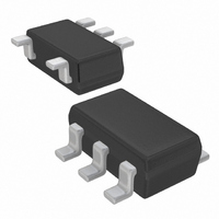
XC9221A095MR Torex Semiconductor Ltd, XC9221A095MR Datasheet

XC9221A095MR
Specifications of XC9221A095MR
Related parts for XC9221A095MR
XC9221A095MR Summary of contents
Page 1
... Externally set (XC9220/XC9221B) : Integral protection (1.0 ms) (XC9220/XC9221 Aand B series) Short-circuit protection : Ceramic capacitor : SOT-25 USP- RoHS Compliant, Pb Free XC9221A095MR (VOUT=3.3V, FOSC=500kHz) CIN=47μF (OS-Con), CL=47μF (OS-Con), L=10μH (CDRH8D43, SUMIDA) VIN=5.0V VIN=16.0V VIN=12. 100 1000 Output Current ...
Page 2
XC9220/XC9221 ■PIN CONFIGURATION V EXT CE SOT-25 (TOP VIEW) ■PIN ASSIGNMENT PIN NUMBER SOT-25 USP- ■PRODUCT CLASSIFICATION ●Ordering ...
Page 3
DIAGRAMS ●XC9220/21A and C series ■ ABSOLUTE MAXIMUM RATINGS PARAMETER V Pin Voltage IN FB Pin Voltage CE/C Pin Voltage SS EXT/ Pin Voltage EXT/ Pin Current SOT-25 Power Dissipation USP-6C Operating Temperature Range Storage Temperature Range ● XC9220/21B ...
Page 4
XC9220/XC9221 ■ELECTRICAL CHARACTERISTICS XC9220/XC9221 A and C series PARAMETER SYMBOL FB Voltage Input Voltage Range UVLO Voltage V (Minimum Operating Voltage) Supply Current 2 Stand-by Current Oscillation Frequency f Maximum Duty Ratio MAXDTY PFM Duty Ratio PFMDTY EXT/ High On ...
Page 5
CHARACTERISTICS (Continued) XC9220/XC9221 B and D series PARAMETER SYMBOL FB Voltage V Input Voltage Range V UVLO Voltage V UVLO (Minimum Operating Voltage) Supply Current 2 I DD2 Stand-by Current I STB Oscillation Frequency F OSC Maximum Duty Ratio ...
Page 6
XC9220/XC9221 ■TYPICAL APPLICATION CIRCUITS ■OPERATIONAL EXPLANATION The XC9220/XC9221 series consists of a reference voltage source, ramp wave circuit, error amplifier, PWM comparator, phase compensation circuit, protection circuits, UVLO circuit and others. The series ICs compare, using the error amplifier, the ...
Page 7
EXPLANATION (Continued) <UVLO (Under Voltage Lock Out) > When the input voltage becomes 2.3V (TYP.) or lower, the external P-channel driver transistor is forced OFF. Once the UVLO operates, the XC9220/XC9221A and C series (soft-start internally set type) resets ...
Page 8
XC9220/XC9221 ■OPERATIONAL EXPLANATION (Continued) <Protection Circuits> 1. Integral Protection Circuit (Latch Type) In the circuit of the XC9220/XC9221 A and B series, the more load current becomes larger, the duty of the EXT/ pin gradually expands, and the duty reaches ...
Page 9
EXPLANATION (Continued) ● Output Voltage Setting Output voltage can be set by adding split resistors. Output voltage is determined by the following equation, based on the values of R and R . The sum of R FB1 FB2 V ...
Page 10
XC9220/XC9221 ■OPERATIONAL EXPLANATION (Continued) ● Setting of Coil Value Recommended inductance value of coil by oscillation frequency is shown in the chart below. fOSC (kHz) 300 500 1000 However, the more current change in each pulse becomes larger, the more ...
Page 11
ON USE 1. The XC9220/XC9221 series are designed for use with an output ceramic capacitor. If, however, the potential difference between input and output is too large, a ceramic capacitor may fail to absorb the resulting high switching energy ...
Page 12
XC9220/XC9221 ■ NOTES ON USE (Continued) ● Instructions on Pattern Layout 1. Wire external components as close to the IC as possible and use thick, short connecting traces to reduce the circuit impedance. 2. Please pay special attention to the ...
Page 13
CIRCUITS Circuit 1: Supply Current, Stand-by Current, CE Current VIN A A CE/CSS CIN:1uF Circuit 3: Oscillation Frequency, PFMDUTY, UVLO, Efficiency Circuit 4: EXT On Resistance, FB Current VIN CIN:1uF CE/CSS Circuit ...
Page 14
XC9220/XC9221 ■TYPICAL PERFORMANCE CHARACTERISTICS (1) Efficiency vs. Output Current XC9220/21x095xx Tr:2SJ646, SBD:DE5PC3, CDRH127-10uH, CIN=10uF(ceramic), CL=44uF(ceramic), RSENSE=50mohm VIN=12V => VOUT=5V 100 0 100 Output Current: IOUT (mA) (2) Output ...
Page 15
PERFORMANCE CHARACTERISTICS (Continued) (4) FB Voltage Temperature Characteristics XC9220/21 Series 1.00 0.95 0.90 0.85 0.80 0.75 -50 - Ambient Temperature ℃ ) (6) Input Voltage Temperature Characteristics XC9220/21 Series VIN=5V, Fosc=300k,500kHz ...
Page 16
XC9220/XC9221 ■TYPICAL PERFORMANCE CHARACTERISTICS (Continued) (10) EXT H ON Resistance Characteristics XC9220/21 Series Input Voltage: VIN (V) (11) Soft-Start Time Temperature Characteristics XC9220/21 Series VIN=5V, Fosc=300k,500kHz 8.0 ...
Page 17
PERFORMANCE CHARACTERISTICS (Continued) (13) Short-Circuit Protection Temperature Characteristics XC9220/21 Series 0.8 0.7 0.6 0.5 0.4 0.3 -50 - Ambient Temperature ℃ ) (15) CE Threshold Temperature Characteristics XC9220/21 Series 1.2 1.0 0.8 0.6 CE_L ...
Page 18
XC9220/XC9221 ■TYPICAL PERFORMANCE CHARACTERISTICS (Continued) (17) Load Transient Response Characteristics XC9220x095xx (500kHz, PWM Control) <External Components> Tr: 2SJ616 (SANYO), SBD: D1FH3 (SHINDENGEN), L=10μH CDRH8D43, SUMIDA) C =47μF (OS-Con), CL=47μF (OS-Con) IN =0.1mA→1000mA ○I OUT V =5.0V, V =3.3V, V =100mV/div., ...
Page 19
INFORMATION ●SOT-25 (SOT-23-5) ●USP-6C XC9220/XC9221 Series 19/22 ...
Page 20
XC9220/XC9221 ■PACKAGING INFORMATION (Continued) ●USP-6C Reference Pattern Layout 20/22 Series ●USP-6C Reference Metal Mask Design ...
Page 21
MARKING RULE ●SOT-25 ① represents product series ② represents product types MARK SOT-25 (TOP VIEW ③ represents oscillation frequency MARK ④ represents production lot number and ...
Page 22
... Should you wish to use the products under conditions exceeding the specifications, please consult us or our representatives assume no responsibility for damage or loss due to abnormal use. 7. All rights reserved. No part of this datasheet may be copied or reproduced without the prior permission of TOREX SEMICONDUCTOR LTD. 22/22 Series ...


