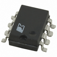
TOP414GN-TL Power Integrations, TOP414GN-TL Datasheet

TOP414GN-TL
Specifications of TOP414GN-TL
Available stocks
Related parts for TOP414GN-TL
TOP414GN-TL Summary of contents
Page 1
TOP412/414 TOPSwitch Family Three-terminal PWM Switch Product Highlights Low Cost Replacement for Discrete Switchers • fewer components - cuts cost, increases reliability • Allows for a smaller and lighter solution under 12 mm height, ...
Page 2
TOP412/414 V C CONTROL Z C SHUNT REGULATOR/ ERROR AMPLIFIER - + 5 OSCILLATOR D MAX CLOCK SAW R E Figure 2. Functional Block Diagram. Pin Functional Description DRAIN Pin: Output MOSFET drain connection. Provides internal bias ...
Page 3
TOPSwitch Family Functional Description TOPSwitch is a self biased and protected linear control current- to-duty cycle converter with an open drain output. High efficiency is achieved through the use of CMOS and integration of the maximum number of functions possible. ...
Page 4
TOP412/414 TOPSwitch Family Functional Description (cont.) The first time V reaches the upper threshold, the high-voltage C current source is turned off and the PWM modulator and output transistor are activated, as shown in Figure 5(a). During normal operation (when ...
Page 5
DRAIN 0 V OUT 0 I OUT Figure 6. Typical Waveforms for (1) Normal Operation, (2) Auto-restart, (3) Latching Shutdown, and (4) Power Down Reset. CONTROL ...
Page 6
TOP412/414 General Circuit Operation Figure 7 shows a typical DC-DC converter application using the TOP414G. This supply delivers and works over a wide input range from 36-72 VDC. The power supply operates at an ambient ...
Page 7
Key Application Issues Use a Kelvin connection to the SOURCE pin for the CONTROL pin bypass capacitor. Use single point grounding techniques at the SOURCE pin as shown in Figure 8. Use a ceramic high frequency decoupling capacitor to bypass ...
Page 8
TOP412/414 DRAIN Voltage ............................................ -0.3 to 350 V CONTROL Voltage ..................................... - 0 Storage Temperature ..................................... -65 to 150 °C Notes: 1. All voltages referenced to SOURCE Normally limited by internal circuitry. 3. 1/16" ...
Page 9
Specification Symbol SHUTDOWN/AUTO-RESTART CONTROL Pin I C Charging Current Charging Current Temperature Drift Auto-restart V Threshold Voltage C(AR) UV Lockout Threshold Voltage Auto-restart Hysteresis Voltage Auto-restart Duty Cycle Auto-restart Frequency CIRCUIT PROTECTION Self-protection I Current Limit LIMIT Leading Edge t ...
Page 10
TOP412/414 Specification Symbol OUTPUT ON-State R Resistance DS(ON) OFF-State I Current DSS Breakdown BV Voltage DSS Rise t Time R Fall t Time F SUPPLY DRAIN Supply Voltage Shunt Regulator V Voltage C(SHUNT) Shunt Regulator Temperature Drift I CD1 CONTROL ...
Page 11
Specification Symbol LOW INPUT VOLTAGE OPERATION (See Note C) DRAIN Supply Voltage CONTROL Pin Charging Current Auto-restart Duty Cycle Auto-restart Frequency NOTES: A. For specifications with negative values, a negative temperature coefficient corresponds to an increase in magnitude with increasing ...
Page 12
TOP412/414 90% DRAIN VOLTAGE 10 Figure 9. TOPSwitch Duty Cycle Measurement. D CONTROL TOPSwitch S NOTES: 1. This test circuit is not applicable for current limit or output characteristic measurements. 2. For P ...
Page 13
BENCH TEST PRECAUTIONS FOR EVALUATION OF ELECTRICAL CHARACTERISTICS The following precautions should be followed when testing TOPSwitch by itself outside of a power supply. The schematic shown in Figure 11 is suggested for laboratory testing of TOPSwitch. When the DRAIN ...
Page 14
TOP412/414 Typical Performance Characteristics (cont.) OUTPUT CHARACTERISTICS 5 T CASE = 25 ° CASE = 100 ° Drain Voltage ( 4/99 Scaling Factors: TOP414 1.00 TOP412 0.67 8 ...
Page 15
D S .004 (.10 - G08A J2 .010 (.25 SMD-8 Heat Sink is 2 oz. Copper As Big As Possible .046 .060 .060 .046 ...
Page 16
... Power Integrations reserves the right to make changes to its products at any time to improve reliability or manufacturability. Power Integrations does not assume any liability arising from the use of any device or circuit described herein, nor does it convey any license under its patent rights or the rights of others. ...


