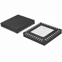
BD95500MUV-E2 Rohm Semiconductor, BD95500MUV-E2 Datasheet

BD95500MUV-E2
Specifications of BD95500MUV-E2
Related parts for BD95500MUV-E2
BD95500MUV-E2 Summary of contents
Page 1
... BD95500MUV ●Description BD95500MUV is a switching regulator with high output current (up to 6A) which can achieve low output voltage (0.7V to 5.0V) from a wide input voltage range (3V to 20V). High efficiency for the switching regulator can be realized by utilizing an internal N-MOSFET power transistor. A new technology called H high transient response against load change ...
Page 2
Absolute Ratings (Ta=25℃) Parameter Input Voltage 1 Input Voltage 2 Input Voltage 3 BOOT Voltage BOOT-SW Voltage LG Voltage REF Voltage Output Voltage ILIM/SS/FS/MODE Voltage VREG Voltage EN Input Voltage Output Current (Average) Power Dissipation 1 Power Dissipation 2 ...
Page 3
CHARACTERISTICS (Unless otherwise noted, Ta=25℃, V Parameter [Whole Device] V Bias Current CC V Bias Current IN V Standby Current CC V Standby Current IN EN Low Voltage EN High Voltage EN Bias Current VREG Voltage [Under Voltage Locked ...
Page 4
Data 2.500 2.498 2.496 2.494 2.492 2.490 - Ta(℃) Fig VREG 2.20 Sweep up 2.15 2.10 2.05 Sweep down 2.00 1.95 1.90 - Ta(℃) Fig ...
Page 5
Data VOUT HG/LG IOUT Fig.13 Transient Response (V =7V) IN VOUT HG/LG IOUT Fig.16 Transient Response (V =7V) IN VOUT IL HG/LG Fig.19 SLLM Mode (I =0A) OUT IL HG/LG/SW Fig.22 Continuous Mode (Io=0A) VOUT HG/LG IOUT Fig.14 Transient ...
Page 6
Data VIN HG/LG VOUT Fig.25 V change IN (5→19V) 1.52 Continuous 1.51 SLLM 1.50 1.49 1.48 0.001 0.01 0.1 1 Iout [A] Fig. OUT OUT VIN HG/LG VOUT Fig.26 V change IN (19→5V) 500 Continuous 400 ...
Page 7
Diagram VDD Vcc 5 EN Reference 39 Block REF×0.85 SS×0.85 Vcc V OUT REF 10 1 Power PGOOD Good SS V OUT 11 EN/UVLO TSD Thermal Protection 6 GND ●Pin Configuration PGND ...
Page 8
... The IC controls the output voltage (REF≒VOUT). ・ILIM (4 Pin) BD95500MUV detects the voltage between Is+ pin and Is- pin and limits the output current (OCP). Voltage equivalent to 1/10 of the ILIM voltage is the voltage drop of external current sense resistor. A very low current sense resistor or inductor DCR can also be used for this platform. ・ ...
Page 9
... Operation The BD95500MUV is a switching regulator controller incorporating ROHM’s proprietary H When V drops due to a rapid load change, the system quickly restores V OUT serves to improve the regulator’s transient response. Activating the Light Load Mode will also exercise Simple Light Load Mode (SLLM) control when the load is light, to further increase efficiency ...
Page 10
Chart ・Soft Start Function OUT I IN ・Soft Stop Function EN T SS(OFF) 1. OUT Tdelay ・Timer Latch Type Short Circuit Protection REF×0.70 V OUT 1ms SCP EN/UVLO Soft start is exercised ...
Page 11
Over Voltage Protection REF×1.2 V OUT HG LG Switching ・Over current protection circuit LIMIT I L ・Synchronous operation with external power supply 3.3V (External Power Supply) 1.5 V (BD95500 Output 1) When ...
Page 12
Component Selection 1. Inductor (L) selection ΔIL VIN VOUT PGND Output Ripple Current ※Passing a current larger than the inductor’s rated current will cause magnetic saturation in the inductor and decrease system efficiency. ...
Page 13
Setting Detection Resistance VIN PGND Is+ Is- Current limit VIN PGND Is+ Is- Current limit I L detect point I LIMIT 0 VIN HG ...
Page 14
VIN=5V 7V 2500 12V 16V 2000 19V 1500 1000 500 100 RFS [kΩ] 1200 1000 800 600 400 200 100 Resistance [kΩ] 6. Setting standard voltage (REF) V REF 3 H ...
Page 15
Setting output voltage This IC is operated that output voltage is REF≒V And it is operated that output voltage is feed back to FB pin in case the output voltage is 0.7V to 2.0V REF H ...
Page 16
Equivalent Circuit 1pin (PGOOD) 7pin (VREG) VCC 10pin (REF) VCC 13pin (Is+) VCC 37pin (VINS) 40pin (MODE) VCC 3pin (CE) VCC 8pin (FS) VCC 11pin (VOUT) VCC 22-29pin (SW) VIN PGND 38pin (BOOT) VDD SW 16/20 4pin (ILIM) VCC ...
Page 17
... R12 10Ω ROHM R13 ROHM R14 1kΩ ROHM R15 1kΩ ROHM R16 100kΩ ROHM SW BD95500MUV VQFN040-V6060 R6 R4 ILIM R8 R9 PGOOD Part Part name No BD95500MUV R17 RB051L-40 R18 CDEP105NP-4R3MC-88 R19 - R20 MCR03 C1 MCR03 C2 MCR03 C3 MCR03 C4 MCR03 C5 MCR03 C6 MCR03 C7 MCR03 C8 MCR03 C9 MCR03 ...
Page 18
... IC off to prevent thermal runaway not designed to protect the IC or guarantee its operation. Do not continue to use the IC after operating this circuit or use the environment where the operation of this circuit is assumed. BD95500MUV (10) Testing on application boards When testing the application board, connecting a capacitor to a pin with low impedance subjects the IC to stress. ...
Page 19
Regarding input pin of the IC This monolithic IC contains P+ isolation and P substrate layers between adjacent elements in order to keep them isolated. P-N junctions are formed at the intersection of these P layers with the N ...
Page 20
Designations (Selections) for Ordering Package Type ・BD95500 ・MUV : VQFN040-V6060 VQFN040-V6060 <Dimension> 6.0±0.1 S 0.08 S 3.7±0.1 C0 +0.05 0.25 0.75 -0.04 0 ...


