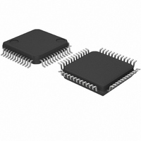
BD9012KV-E2 Rohm Semiconductor, BD9012KV-E2 Datasheet

BD9012KV-E2
Specifications of BD9012KV-E2
Available stocks
Related parts for BD9012KV-E2
BD9012KV-E2 Summary of contents
Page 1
... BD9012KV ●Overview The BD9012KV is a 2-ch synchronous controller with rectification switching for enhanced power management efficiency. It supports a wide input range, enabling low power consumption ecodesign for an array of electronics. ●Features 1) Wide input voltage range: 4.5V to 30V 2) Precision voltage references: 0.8V±1% ...
Page 2
Parameter Input voltage 1 Input voltage 2 BOOT-SW voltage BOOT-SW Carrier frequency Synchronous frequency Synchronous pulse duty Min OFF pulse ★This product is not designed to provide resistance against radiation. *1 After more than 4.5V, voltage range. ...
Page 3
Ta=25℃) 100 5. 3. VIN=12V OUTPUT CURRENT:Io[A] Fig.1 Efficiency 1 0.816 0.812 0.808 0.804 0.800 0.796 0.792 0.788 0.784 -40 -15 10 ...
Page 4
VREG5 44 5 VCCCL2 CL2 3 BOOT2 2 1 OUTH2 48 SW2 OUTL2 46 DGND2 47 39 FB2 SS2 37 COMP2 38 SYNC EXTVCC STB VCC Reg B.G SYNC UVLO TSD ...
Page 5
SS2 37 COMP2 38 FB2 39 N.C 40 EXTVCC 41 N.C 42 N.C 43 VREG5 44 N.C 45 OUTL2 46 DGND2 47 SW2 Fig-15 ●Block ...
Page 6
VQFP48C pin numbers) SP8K2 (SLF10145:TDK) Vo(1.8V/2A) 10uH RB051 L-40 3300pF 15k Ω 30uF 150 Ω (C2012JB 0J106K :TDK) 12k Ω 10000pF 1k Ω 0.1uF There are many factors(The PCB board layout, Output Current, etc.)that can ...
Page 7
Setting the output L value ΔI L Fig-17 VCC I L VOUT L Co Fig-18 Output ripple current ※Outputting a current in excess of the coil current rating will cause magnetic saturation of the coil and ...
Page 8
Feedback resistor design Please refer to the following equation in determining the proper feedback resistance. The recommended setting range between 10kΩ and 330kΩ. Resistance less than 10kΩ risks decreased power efficiency, while setting the resistance value ...
Page 9
Setting over current detection values The current limit value(ILimit)is determined by the resistance of the RCL established between CL and VCCCL. VIN VCCCL RCL Fig-23 When the current goes beyond the threshold value, the ...
Page 10
When electrolytic or other high-ESR output capacitors are used: Phase compensation is relatively simple for applications employing high-ESR output capacitors (on the order of several Ω). In DC/DC converter applications, where LC resonance circuits are always incorporated, the phase margin ...
Page 11
GSM1 GSM2 Fig-33 (10)Schottky barrier diode selection V CC Fig-34 (11)Sequence function ●Circuit diagram VCC VREG5 OUTH1 BOOT1 VCC BOOT2 Vo1 SW1 OUTL1 DGND1 FB1 COMP1 SS1 DET2 STB EN1 ...
Page 12
BOOT OUTH SW 300k 34PIN(SYNC) VREG5 5k SYNC 250k 1P 25,26,27PIN (STB,EN1,EN2) VCC STB EN 172.2k 100k 135.8k 35PIN(LLM) VREG5A LLM 308k 41PIN(EXTVCC) 44PIN(VREG5) VCC EXTVCC VCC 150k VREG5 746.32k 255k 14,47PIN(DGND1,DGND2) 15,46PIN(OUTL1,OUTL2) 44,17PIN(VREG5,VREG5A) ...
Page 13
Exceeding the absolute maximum ratings for supply voltage, operating temperature or other parameters can damage or destroy the IC. When this occurs impossible to identify the source of the damage as a short ...
Page 14
In order to avoid these problems, limiting output pin capacitance to 100μF or less and inserting a Vcc series countercurrent prevention diode or bypass diode between the various pins and the Vcc is recommended. Countercurrent prevention diode 11)Thermal shutdown (TSD) ...
Page 15
Output When each function operates, each output is as follows. Function Upper side FET EN= L OFF OCP OFF UVLO OFF TSD OFF OUTH Lower side FET OUTL L OFF OFF L L ...
Page 16
VQFP48C PD(W) 1.2 1.0 0.8 0.6 ①0.75W 0.4 0.2 0 AMBIENT TEMPERATORE:Ta [℃] ①:Stand-alone IC ②:Mounted on Rohm standard board (70mm x 70mm x 1.6mm glass-epoxy board ) ●Part order number B ...
Page 17
Appendix No technical content pages of this document may be reproduced in any form or transmitted by any means without prior permission of ROHM CO.,LTD. The contents described herein are subject to change without notice. The specifications for the product ...


