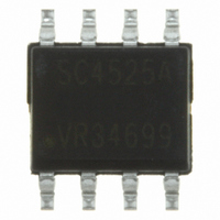
SC4525ASETRT Semtech, SC4525ASETRT Datasheet - Page 12

SC4525ASETRT
Manufacturer Part Number
SC4525ASETRT
Description
IC STEP-DWN SW REG 3A 28V 8-SOIC
Manufacturer
Semtech
Type
Step-Down (Buck)r
Datasheet
1.SC4525ASETRT.pdf
(19 pages)
Specifications of SC4525ASETRT
Internal Switch(s)
Yes
Synchronous Rectifier
No
Number Of Outputs
1
Current - Output
3A
Frequency - Switching
300kHz ~ 1.3MHz
Voltage - Input
8 ~ 28 V
Operating Temperature
-40°C ~ 125°C
Mounting Type
Surface Mount
Package / Case
8-SOIC
Lead Free Status / RoHS Status
Lead free / RoHS Compliant
Voltage - Output
-
Power - Output
-
Other names
SC4525ASETR
Available stocks
Company
Part Number
Manufacturer
Quantity
Price
Company:
Part Number:
SC4525ASETRT
Manufacturer:
Semtech
Quantity:
5 650
Part Number:
SC4525ASETRT
Manufacturer:
SEMTECH/美国升特
Quantity:
20 000
Applications Information (Cont.)
diodes should have an average forward current rating
at least 3A and a reverse blocking voltage of at least a
few volts higher than the input voltage. For switching
regulators operating at low duty cycles (i.e. low output
voltage to input voltage conversion ratios), it is beneficial
to use freewheeling diodes with somewhat higher
average current ratings (thus lower forward voltages). This
is because the diode conduction interval is much longer
than that of the transistor. Converter efficiency will be
improved if the voltage drop across the diode is lower.
The freewheeling diode should be placed close to the
SW pin of the SC4525A to minimize ringing due to trace
inductance. 20BQ030 (International Rectifier), B320A,
B330A (Diodes Inc.), SS33 (Vishay), CMSH3-20MA and
CMSH3-40MA (Central-Semi.) are all suitable.
The freewheeling diode should be placed close to the SW
pin of the SC4525A on the PCB to minimize ringing due to
trace inductance.
Bootstrapping the Power Transistor
The minimum BST-SW voltage required to fully saturate
the power transistor is shown in Figure 4, which is about
.98V at room temperature.
The BST-SW voltage is supplied by a bootstrap circuit
powered from either the input or the output of the
converter (Figure 5). To maximize efficiency, tie the
bootstrap diode to the converter output if V
Since the bootstrap supply current is proportional to the
converter load current (Equation (0), page 4), using a
lower voltage to power the bootstrap circuit reduces
driving loss and improves efficiency.
For the bootstrap circuit, a fast switching PN diode (such
as N448 or N94) and a small (0.µF – 0.47µF) ceramic
capacitor is sufficient for most applications. When
bootstrapping from 2.5V to 3.0V output voltages, use a
low forward drop Schottky diode (BAT-54 or similar) for
D
reduce the maximum BST voltage by connecting a Zener
diode (D
. When bootstrapping from high input voltages (>20V),
3
) in series with D
VIN
VIN
.
IN
IN
SC4525A
SC4525A
BST
BST
GND
GND
SW
SW
(a)
(a)
D
D
2
2
C1
C1
O
D1
D1
>2.5V.
VOUT
VOUT
Figure 5. Typical Minimum Bootstrap Voltage required
Loop Compensation
The goal of compensation is to shape the frequency
response of the converter so as to achieve high DC
accuracy and fast transient response while maintaining
loop stability.
SS270 REV 6-7
SS270 REV 6-7
Figure 6. Methods of Bootstrapping the SC4525A
VIN
VIN
VIN
VIN
to Saturate Transistor (I
2.2
2.2
2.1
2.1
2.0
2.0
1.9
1.9
1.8
1.8
1.7
1.7
1.6
1.6
-50
-50
D3
D3
IN
IN
IN
IN
Minimum Bootstrap Voltage
Minimum Bootstrap Voltage
I
I
SW
SW
-25
-25
SC4525A
SC4525A
SC4525A
SC4525A
=-3.9A
=-3.9A
D1
D1
BST
BST
GND
GND
BST
BST
GND
GND
vs Temperature
vs Temperature
Temperature (
Temperature (
0
0
SW
SW
SW
SW
25
25
(a)
(a)
(b)
(b)
50
50
D
D
o
o
D
D
2
2
C)
C)
SW
75
75
2
2
C1
C1
C1
C1
= -3.9A)
D1
D1
100 125
100 125
VOUT
VOUT
VOUT
VOUT
2
VIN
VIN
D3
D3


