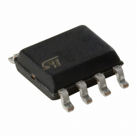
L6726ATR STMicroelectronics, L6726ATR Datasheet - Page 17

L6726ATR
Manufacturer Part Number
L6726ATR
Description
IC CTRLR PWM SGL PHASE 8-SOIC
Manufacturer
STMicroelectronics
Type
Step-Down (Buck)r
Datasheet
1.L6726ATR.pdf
(35 pages)
Specifications of L6726ATR
Internal Switch(s)
No
Synchronous Rectifier
No
Number Of Outputs
1
Voltage - Output
Adj to 0.8V
Frequency - Switching
270kHz
Voltage - Input
1.5 ~ 12 V
Operating Temperature
-20°C ~ 85°C
Mounting Type
Surface Mount
Package / Case
8-SOIC (3.9mm Width)
Output Current
1.5 A
Input Voltage
4.1 V to 13.2 V
Operating Temperature Range
- 40 C to + 150 C
Mounting Style
SMD/SMT
For Use With
497-9046 - BOARD EVAL BASED ON L6726A497-6364 - BOARD DEMO FOR TS4995EIJT497-6259 - BOARD EVAL 1PH STPDN CONV L6726A
Lead Free Status / RoHS Status
Lead free / RoHS Compliant
Current - Output
-
Power - Output
-
Lead Free Status / Rohs Status
Lead free / RoHS Compliant
Other names
497-5906-2
Available stocks
Company
Part Number
Manufacturer
Quantity
Price
Company:
Part Number:
L6726ATR
Manufacturer:
FUJI
Quantity:
130
Part Number:
L6726ATR
Manufacturer:
ST
Quantity:
20 000
L6726A
Type II compensation relies on the zero introduced by the output capacitors bank to achieve
stability. Thus, a needed condition to successfully apply type II compensation is
(usually true when output capacitor is based on electrolytic, aluminium electrolytic or
tantalum capacitor).
To define compensation network components values, the below suggestions may be
followed:
a)
b)
c)
d)
e)
f)
Set the output resistor divider in order to obtain the desired output voltage:
Usual values of R
(consider trade-off between power dissipation on output resistor divider and offset
introduced by FB bias current).
If the desired output voltage is equal to internal reference, R
FB pin can be directly connected to V
Set R
the approximated formula:
If V
Place F
Place F
Check that compensation network gain is lower than open loop transconductance
EA gain.
Estimate phase margin obtained (it should be greater than 45°) and repeat,
modifying parameters, if necessary.
C
OUT
R
F
---------- -
R
R
C
F
F
OS
FB
=
P
in order to obtain the desired closed loop regulator bandwidth according to
Z
P
= V
=
=
-------------------------------- -
2π R
below F
at 0.5
=
F
------------------------------ -
----------------------------------------------------
π R
REF
0dB
⋅
V
-------------- 1
V
⋅
OUT
REF
F
5
F
, just consider (R
⋅
·
2
LC
F
⋅
F
F
⋅
F
LC
SW
ESR
FB
–
C
LC
C
F
(typically 0.2
:
F
and R
Doc ID 12754 Rev 4
⋅
⋅
F
ΔV
------------------ -
SW
V
OSC
IN
–
OS
1
≅
⋅
ranges from some hundreds of Ω to some kΩ
------- -
gm
------------------------------ -
π R
FB
1
·
⋅
F
+R
⋅
LC
R
----------------------------
F
1
OS
FB
⋅
):
OUT
F
R
SW
)/R
+
OS
.
R
OS
OS
factor equal to 1.
OS
Application details
has to be NC and
F
ESR
<
F
17/35
0dB


