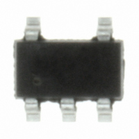
ST1S12G12R STMicroelectronics, ST1S12G12R Datasheet - Page 6

ST1S12G12R
Manufacturer Part Number
ST1S12G12R
Description
IC DC-DC CONN STDN 1.2V TSOT23-5
Manufacturer
STMicroelectronics
Type
Step-Down (Buck)r
Datasheet
1.ST1S12G18R.pdf
(20 pages)
Specifications of ST1S12G12R
Internal Switch(s)
Yes
Synchronous Rectifier
Yes
Number Of Outputs
1
Voltage - Output
1.2V
Current - Output
700mA
Frequency - Switching
1.7MHz
Voltage - Input
2.5 ~ 5.5 V
Operating Temperature
-40°C ~ 85°C
Mounting Type
Surface Mount
Package / Case
TSOT-23-5, TSOT-5, TSOP-5
Output Voltage
1.2 V
Output Current
0.7 A
Input Voltage
2.5 V to 5.5 V
Switching Frequency
1.7 MHz
Operating Temperature Range
- 40 C to + 125 C
Mounting Style
SMD/SMT
Duty Cycle (max)
100 %
For Use With
497-8220 - BOARD EVAL BASED ON ST1S12497-8219 - BOARD EVAL BASED ON ST1S12
Lead Free Status / RoHS Status
Lead free / RoHS Compliant
Power - Output
-
Lead Free Status / Rohs Status
Lead free / RoHS Compliant
Other names
497-6905-2
ST1S12G12R
ST1S12G12R
Available stocks
Company
Part Number
Manufacturer
Quantity
Price
Part Number:
ST1S12G12R
Manufacturer:
ST
Quantity:
20 000
Electrical characteristics
4
Table 6.
1. Guaranteed by design, but not tested in production.
6/20
%V
R
%V
R
%V
%V
Symbol
PWMf
T
DSON
DSON
D
T
I
V
SHDN
V
I
O
SWL
FB
I
MAX
HYS
I
I
O
O
O
EN
FB
EN
ν
Q
O
IN
/ΔV
/ΔI
/ΔI
/ΔI
-N NMOS switch on resistance
-P PMOS switch on resistance
S
O
O
O
IN
Feedback voltage
V
Minimum input voltage
Quiescent current
Output current
Enable threshold
Enable pin current
Reference line regulation
Reference load regulation
PWM switching frequency
Maximum duty cycle
Switching current limitation
Efficiency
Thermal shutdown
Thermal shutdown hysteresis
Load transient response
Short circuit removal
response
Electrical characteristics
V
otherwise specified. Typical values are referred to 25 °C).
Electrical characteristics for ST1S12G
FB
IN
pin bias current
= V
EN
Parameter
(1)
= 3.6 V, C
IN
= 4.7 µF, C
T
I
V
V
V
Device ON, V
Device OFF
V
I
I
I
(1)
I
I
I
t
I
T
O
O
SW
SW
O
O
O
R
O
A
J
IN
EN
IN
IN
= 100mA to 700mA, T
= t
= 10mA to 0.7A
= 10 mA to 700mA
= 10mA to 100 mA, V
= 100mA to 0.7A, V
= 10mA to I
= -40 to 125°C
= 25°C
Doc ID 14314 Rev 3
= 2.5V to 5.5 V
= 2.5V to 5.5V
= V
= 100mA
= 100mA
= 0, T
F
≥ 200ns, C
O
EN,
Test conditions
= 10 µF, L = 2.2 µH, T
J
(1)
V
= -40°C to 85°C
FB
IN
O
= 0.65V
= short,
= 2.5V to 5.5V
O
(1)
=22µF
(1)
(1)
O
O
A
= 1.8V
ST1S12XX, ST1S12XX12, ST1S12XX18
= 25°C
(1)
= 1.8V
J
= - 40 to 125 °C (unless
Min.
1.16
582
130
-50
2.5
0.7
1.5
-10
-5
0.0025 0.005 %V
Typ.
0.05
0.25
0.25
600
500
150
1.7
1.6
80
90
15
Max.
2.08
0.45
618
600
100
+10
0.5
0.1
0.4
50
+5
1
1
%V
%V
%V
MHz
Unit
O
nA
µA
µA
µA
°C
°C
O
%
%
Ω
Ω
V
V
A
V
A
/ΔV
/mA
O
O
IN


