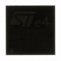
ST1S10PUR STMicroelectronics, ST1S10PUR Datasheet - Page 6

ST1S10PUR
Manufacturer Part Number
ST1S10PUR
Description
IC REG STEPDOWN 3A 900KHZ DFN8
Manufacturer
STMicroelectronics
Type
Step-Down (Buck)r
Datasheet
1.ST1S10PUR.pdf
(26 pages)
Specifications of ST1S10PUR
Internal Switch(s)
Yes
Synchronous Rectifier
Yes
Number Of Outputs
1
Voltage - Output
0.8 ~ 15.3 V
Current - Output
3A
Frequency - Switching
900kHz
Voltage - Input
2.5 ~ 18 V
Operating Temperature
-25°C ~ 125°C
Mounting Type
Surface Mount
Package / Case
8-DFN
Output Voltage
0.8 V to 15.3 V
Output Current
3 A
Input Voltage
2.5 V to 18 V
Switching Frequency
0.9 MHz
Operating Temperature Range
- 25 C to + 125 C
Mounting Style
SMD/SMT
Duty Cycle (max)
90 %
For Use With
497-8407 - BOARD EVAL STP04CM05/ST1S10497-8216 - BOARD EVAL BASED ON ST1S10497-8229 - BOARD EVAL BASED ON ST1S10
Lead Free Status / RoHS Status
Lead free / RoHS Compliant
Power - Output
-
Lead Free Status / Rohs Status
Lead free / RoHS Compliant
Other names
497-6313-2
Available stocks
Company
Part Number
Manufacturer
Quantity
Price
Company:
Part Number:
ST1S10PUR
Manufacturer:
ST
Quantity:
12 025
Company:
Part Number:
ST1S10PUR
Manufacturer:
STMicroelectronics
Quantity:
118 692
Part Number:
ST1S10PUR
Manufacturer:
ST
Quantity:
20 000
Electrical characteristics
4
Table 5.
6/26
%V
V
V
@I
V
SYNC
OUT
OUT
V
R
R
Symbol
%V
PWM fs
T
F
IH_SYNC
IL_SYNC
ΔI
OUT
D
DSon
DSon
T
O
V
I
I
V
I
SHDN
SYNC
SWL
OUT
I
INH
MAX
HYS
I
=short
FB
OUT
INH
ν
/ΔI
/ΔI
OUT
FB
Q
/ΔV
WD
-N
-P
OUT
OUT
/
IN
Electrical characteristics
V
+0.1 µF, C
the typical application circuit. Typical values assume T
Electrical characteristics
Feedback voltage
V
Quiescent current
Output current
Inhibit threshold
Inhibit pin current
Reference line regulation
Reference load regulation
PWM switching frequency
Maximum duty cycle
NMOS switch on resistance
PMOS switch on resistance
Switch current limitation
Efficiency
Thermal shut down
Thermal shut down hysteresis
Output transient response
Short circuit removal response
(overshot)
SYNC frequency capture range
SYNC pulse width
SYNC input threshold low
SYNC input threshold high
IN
FB
= V
pin bias current
IN_SW
OUT
Parameter
= V
(1)
= 22 µF, L1 = 3.3 µH, T
IN_A
(2)
= V
INH
= 12 V, V
Doc ID 13844 Rev 4
T
T
V
V
V
V
Device ON
Device OFF
2.5 V < V
10 mA < I
V
T
I
I
I
I
100 mA < I
t
10 mA < I
V
V
V
V
V
SW
SW
OUT
OUT
R
J
J
INH
INH
IN
OUT
FB
J
IN
SYNC
IN
IN
IN
= t
= 25°C
= -25°C to 125°C
= 25°C
= 2.5 V to 18 V,
= 2.5 V to 18 V
= 2.5 V to 18 V
= 2.5 V to 18 V
= 2.5 V to 18 V
= 750 mA
= 750 mA
= 0.7 V, Sync = GND
SYNC
J
= 100 mA to 300 mA
= 300 mA to 3 A
F
> 1.2 V, not switching
< 0.4 V
Test conditions
= 0.8 V to 13.6 V
= -25 to 125°C (Unless otherwise specified, refer to
≥ 500 ns
= 0 to 5 V
IN
OUT
OUT
OUT
= GND, V
< 18 V
< short
< 3 A
< 1 A,
OUT
J
(2)
= 25°C).
= 5 V, I
Min.
784
776
250
3.0
1.2
0.7
0.4
1.6
85
OUT
= 10 mA, C
Typ.
0.10
0.12
800
800
150
±10
1.5
0.4
0.5
0.9
5.0
90
85
90
15
±5
2
2
Max.
816
824
600
2.5
0.4
1.1
1.2
0.4
6
IN
= 4.7 µF
%V
%V
ST1S10
ΔI
%V
%V
ΔV
MHz
MHz
Unit
mV
mV
mA
nA
µA
µA
°C
°C
ns
OUT
%
%
%
A
V
V
Ω
Ω
V
V
A
OUT
OUT
IN
O
O
/
/


