LM3370SD-3021/NOPB National Semiconductor, LM3370SD-3021/NOPB Datasheet
LM3370SD-3021/NOPB
Specifications of LM3370SD-3021/NOPB


Related parts for LM3370SD-3021/NOPB


LM3370SD-3021/NOPB Summary of contents
Page 1
... Default fixed voltages for the 2 output voltages combination can be customized to fit system requirements by contacting National Semiconductor Corporation. Typical Performance Curve Efficiency vs. Output Current, V © 2008 National Semiconductor Corporation Features ■ compatible interface — V OUT1 — ...
Page 2
Typical Application Functional Block Diagram www.national.com FIGURE 1. Typical Application Circuit FIGURE 2. Functional Diagram 2 20167301 20167302 ...
Page 3
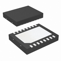
Package Marking Information 16-Lead LLP Package FIGURE 3. Top Marking Pin Descriptions (LLP) Pin # Name 1 V IN2 2 SW2 3 PGND2 SGND 6 PGND1 7 SW1 8 V IN1 9 FB1 10 SDA 11 ...
Page 4
Package Marking Information (micro SMD) 20167377 Top View Pin Descriptions (micro SMD) Pin # Name A1 SW1 A2 V IN1 A3 SGND A4 FB1 B1 PGND1 B2 PGND1_S B3 SDA B4 SCL SGND C3 nPOR1 C4 ...
Page 5
... Buck 1 & Buck 2 Ordering Information (LLP) Order Number Voltage Option LM3370SD-3013 LM3370SDX-3013 LM3370SD-3021 LM3370SDX-3021 LM3370SD-3416 LM3370SDX-3416 LM3370SD-3621 LM3370SDX-3621 LM3370SD-3806 LM3370SDX-3806 LM3370SD-4221 LM3370SDX-4221 (micro SMD) Order Number LM3370TL-3607 NOPB LM3370TLX-3607 NOPB LM3370TL-3008 NOPB LM3370TLX-3008 NOPB LM3370TL-3006 NOPB LM3370TLX-3006 NOPB LM3370TL-3806 NOPB LM3370TLX-3806 NOPB ...
Page 6
... Absolute Maximum Ratings If Military/Aerospace specified devices are required, please contact the National Semiconductor Sales Office/ Distributors for availability and specifications VDD to PGND & IN1 IN2 SGND PGND to SGND SDA, SCL, EN, EN2, nPOR1, nPOR2, SW1, SW2, FB1 & FB2 (GND - 0. Maximum Continuous Power ...
Page 7
... J Note 4: For detailed soldering specifications and information, please refer to National Semiconductor Application Note 1187: Leadless Leadframe Package (LLP) (AN-1187). Note 5: The Human body model is a 100 pF capacitor discharged through a 1.5 kΩ resistor into each pin. (MIL-STD-883 3015.7) The machine model is a 200 pF capacitor discharged directly into each pin ...
Page 8
... L = 2,2 µH (NR3015T2R2M), C OUT2 IQ_PFM (Non Switching) Both Channels IQ_PWM (Switching) Both Channels R (PFET) vs. Temperature DS_ON V = 3.6V IN www.national.com LM3370SD/TL, Circuit of Figure 4.7 µF (0805) and µF (0805) & OUT IQ_PWM (Non Switching) 20167357 IQ_SD (EN1 = EN2 = 0V) 20167359 R DS_ON 20167346 8 = 3.6V 1.5V & ...
Page 9
R (LLP) vs. V DS_ON IN 20167348 Switching Frequency vs 20167360 Efficiency vs. Output Current Forced PWM Mode 1.2V OUT1 20167362 Current Limit vs. V Output Voltage vs. Output Current V = 3.6V (Forced PWM) IN ...
Page 10
Efficiency vs. Output Current Auto Mode, V OUT1 Efficiency vs. Output Current Auto Mode, V OUT2 Typical Operation Waveform V = 3.6V 1.8V & OUT1 Load = 400 mA www.national.com = 1.5V 20167380 = 3.3V 20167367 ...
Page 11
Typical Operation Waveform V = 3.6V 1.5V 2.5V, IN OUT1 OUT2 Load = 600 mA Each Start-up at PWM for BUCK2 ( V = 3.6V 2.5V, Load = 200 OUT Line ...
Page 12
Load Transient in PFM MODE ( V = 1.5V ) OUT1 Load Transient in PFM MODE ( V Load Transient in PWM MODE ( V = 3.6V OUT1 www.national.com 20167333 = 1.8V ) OUT1 20167335 = 1.5V ) ...
Page 13
Spread Spectrum Enabling ( V Signal at 2 MHz) OUT 20167375 V Stepping OUT ( From 3.3V to 1.8V ) 20167372 V Stepping OUT ( From 1. 20167371 www.national.com ...
Page 14
Operation Description DEVICE INFORMATION The LM3370, a dual high efficiency step down DC-DC con- verter, delivers regulated voltages from input rails between 2.7V to 5.5V. Using voltage mode architecture with syn- chronous rectification, the LM3370 has the ability to deliver ...
Page 15
FORCED PWM MODE The LM3370 auto mode can be bypassed by forcing the de- vice to operate in PWM mode, this can be implemented through the compatible interface, see Table 1. SOFT-START The LM3370 has a soft ...
Page 16
Compatible Interface Electrical Specifications Unless otherwise noted 2.7V to 5.5V. Typical values and limits appearing in normal type apply for T BATT appearing in boldface type apply over the entire junction temperature range for operation, ...
Page 17
TRANSFERRING DATA Every byte put on the SDA line must be eight bits long, with the most significant bit (MSB) being transferred first. The number of bytes that can be transmitted per transfer is unre- stricted. Each byte of data ...
Page 18
Device Register Information Register Information Register Name Location Control 00 Buck 1 01 Buck CHIP ADDRESS INFORMATION REGISTER 00 www.national.com Type R/W Control signal for Buck 1 and Buck 2 R/W Output setting & Mode ...
Page 19
REGISTER 01 REGISTER 02 19 20167312 20167313 www.national.com ...
Page 20
TABLE 1. Output Selection Table via I Data Code 00000 00001 00010 00011 00100 00101 00110 00111 01000 01001 01010 01011 01100 01101 01110 01111 10000 10001 10010 10011 10100 10101 10110 10111 11000 11001 * Can be trimmed at ...
Page 21
... TYP Please refer to for programming the desire output voltage. If the compatible feature is not used, the default output volt- age will be the pre-trimmed voltage. For example, LM3370SD-3021 refers to 1.2V for Buck 1 and 3.3V for Buck 2. V Pin the power supply to the internal control circuit ...
Page 22
The output filter capacitor smoothes out current flow from the inductor to the load, helps maintain a ...
Page 23
... Micro SMD PACKAGE ASSEMBLY AND USE Use of the Micro SMD package requires specialized board layout, precision mounting and careful re-flow techniques, as detailed in National Semiconductor Application Note 1112. Refer to the section "Surface Mount Technology (SMD) As- sembly Considerations". For best results in assembly, align- ment ordinals on the PC board should be used to facilitate placement of the device ...
Page 24
... Physical Dimensions NOTES: UNLESS OTHERWISE SPECIFIED 1. For solder thickness and composition, see “Solder Information” in the packaging section of the National Semiconductor Web Page (www.national.com) 2. Maximum allowable metal burn on lead tips at the package edges is 76 microns. No JEDEC registration as of December 2004. 3. www.national.com ...
Page 25
... NOTE: UNLESS OTHERWISE SPECIFIED 1. EPOXY COATING 2. FOR SOLDER BUMP COMPOSITION, SEE “SOLDER INFORMATION” IN THE PACKAGE SECTION OF THE NATIONAL SEMICONDUCTOR WEB PAGE (www.national.com) 3. RECOMMEND NON-SOLDER MASK DEFINED LANDING PAD. 4. PIN A1 IS ESTABLISHED BY LOWER LEFT CORNER WITH RESPECT TO TEXT ORIENTATION. 5. XXX IN DRAWING NUMBER REPRESENTS PACKAGE SIZE VARIATION WHERE X1 IS PACKAGE WIDTH PACKAGE LENGTH AND X3 IS PACK- AGE HEIGHT ...
Page 26
... For more National Semiconductor product information and proven design tools, visit the following Web sites at: Products Amplifiers www.national.com/amplifiers Audio www.national.com/audio Clock Conditioners www.national.com/timing Data Converters www.national.com/adc Displays www.national.com/displays Ethernet www.national.com/ethernet Interface www.national.com/interface LVDS www.national.com/lvds Power Management www.national.com/power Switching Regulators www.national.com/switchers LDOs www ...