LM22674MRE-5.0/NOPB National Semiconductor, LM22674MRE-5.0/NOPB Datasheet
LM22674MRE-5.0/NOPB
Specifications of LM22674MRE-5.0/NOPB
Available stocks


Related parts for LM22674MRE-5.0/NOPB


LM22674MRE-5.0/NOPB Summary of contents
Page 1
... The LM22674 series also has built in thermal shutdown, current limiting and an enable control input that can power down the regulator to a low 25 µA quiescent current standby condition. Simplified Application Schematic © 2010 National Semiconductor Corporation LM22674/LM22674Q Features ■ Wide input voltage range: 4.5V to 42V ■ ...
Page 2
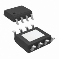
... Connection Diagram Ordering Information Output Order Number Voltage ADJ LM22674MR-ADJ ADJ LM22674MRE-ADJ ADJ LM22674MRX-ADJ PSOP-8 Exposed Pad 5.0 LM22674MR-5.0 5.0 LM22674MRE-5.0 5.0 LM22674MRX-5.0 ADJ LM22674QMR-ADJ ADJ LM22674QMRE-ADJ ADJ LM22674QMRX-ADJ PSOP-8 Exposed Pad 5.0 LM22674QMR-5.0 5.0 LM22674QMRE-5.0 5.0 LM22674QMRX-5.0 *Automotive Grade (Q) product incorporates enhanced manufacturing and support processes for the automotive market, including defect detection methodologies. ...
Page 3
... Absolute Maximum Ratings If Military/Aerospace specified devices are required, please contact the National Semiconductor Sales Office/ Distributors for availability and specifications. VIN to GND EN Pin Voltage SW to GND (Note 2) BOOT Pin Voltage FB Pin Voltage Power Dissipation Electrical Characteristics junction temperature (T ) range of -40°C to +125°C. Minimum and Maximum limits are guaranteed through test, design, or statistical J correlation ...
Page 4
Note 1: Absolute Maximum Ratings indicate limits beyond which damage to the device may occur, including inoperability and degradation of device reliability and/or performance. Functional operation of the device and/or non-degradation at the Absolute Maximum Ratings or other conditions beyond ...
Page 5
Feedback Bias Current vs Temperature Standby Quiescent Current vs Input Voltage Normalized Feedback Voltage vs Input Voltage Normalized Enable Threshold Voltage vs Temperature 30076905 Normalized Feedback Voltage vs Temperature 30076906 30076909 5 30076910 30076907 www.national.com ...
Page 6
Typical Application Circuit and Block Diagram www.national.com FIGURE 1. 3. 500 mA OUT 6 30076914 ...
Page 7
Detailed Operating Description The LM22674 switching regulator features all of the functions necessary to implement an efficient high voltage buck regu- lator using a minimum of external components. This easy to use regulator integrates a 42V N-Channel switch with an ...
Page 8
FIGURE 2. Output Current in Foldback vs. Nominal Duty Cycle The percentage of output current limit fold back is affected by duty cycle, inductance, and See Figure 2 for details. The current limit will only protect the inductor from a ...
Page 9
Generally, calculation as well as simulation can only aid in selecting good power stage components. A good design prac- tice is to test for stability with load transient tests or loop measurement tests. Application note AN-1889 shows how to easily ...
Page 10
FB pin. Other output voltages can use the -ADJ option with a resistor divider. The resistor values can be determined by the following equa- tions: -ADJ option: -5.0 option: Where V = 1.285V typical for the -ADJ ...
Page 11
Thermal Considerations The two highest power dissipating components are the re- circulating diode and the LM22674 regulator IC. The easiest method to determine the power dissipation within the LM22674 is to measure the total conversion losses (Pin – Pout) then ...
Page 12
PCB Layout Example Schematic for Buck/Boost (Inverting) Application See AN-1888 for more information on the inverting (buck- boost) application generating a negative output voltage from a positive input voltage. www.national.com 30076941 30076926 12 ...
Page 13
Physical Dimensions inches (millimeters) unless otherwise noted 8-Lead Plastic PSOP-8 Package NS Package Number MRA08B 13 www.national.com ...
Page 14
... For more National Semiconductor product information and proven design tools, visit the following Web sites at: www.national.com Products Amplifiers www.national.com/amplifiers Audio www.national.com/audio Clock and Timing www.national.com/timing Data Converters www.national.com/adc Interface www.national.com/interface LVDS www.national.com/lvds Power Management www.national.com/power Switching Regulators www.national.com/switchers LDOs www.national.com/ldo LED Lighting www ...