LM22670TJE-5.0/NOPB National Semiconductor, LM22670TJE-5.0/NOPB Datasheet
LM22670TJE-5.0/NOPB
Specifications of LM22670TJE-5.0/NOPB
Available stocks


Related parts for LM22670TJE-5.0/NOPB


LM22670TJE-5.0/NOPB Summary of contents
Page 1
... The LM22670 series also has built in thermal shut- down, current limiting and an enable control input that can power down the regulator to a low 25 µA quiescent current standby condition. Simplified Application Schematic © 2011 National Semiconductor Corporation LM22670/LM22670Q Features ■ Wide input voltage range: 4.5V to 42V ■ ...
Page 2
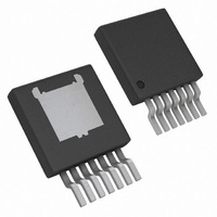
... LM22670MR-ADJ PSOP-8 Exposed Pad ADJ LM22670MRE-ADJ ADJ LM22670MRX-ADJ ADJ LM22670QMR-ADJ ADJ LM22670QMRE-ADJ ADJ LM22670QMRX-ADJ ADJ LM22670TJE-ADJ TO-263 THIN Exposed ADJ LM22670TJ-ADJ ADJ LM22670QTJE-ADJ ADJ LM22670QTJ-ADJ www.national.com 8-Lead Plastic PSOP-8 Package NS Package Number MRA08B 7-Lead Plastic TO-263 THIN Package NS Package Number TJ7A ...
Page 3
... LM22670MRX-5.0 5.0 LM22670QMR-5.0 5.0 LM22670QMRE-5.0 5.0 LM22670QMRX-5.0 5.0 LM22670TJE-5.0 TO-263 THIN Exposed 5.0 LM22670TJ-5.0 5.0 LM22670QTJE-5.0 5.0 LM22670QTJ-5.0 *Automotive Grade (Q) product incorporates enhanced manufacturing and support processes for the automotive market, including defect detection methodologies. Reliability qualification is compliant with the requirements and temperature grades defined in the AEC-Q100 standard. Automotive grade products are identified with the letter Q ...
Page 4
Pin Descriptions Pin Numbers Pin Numbers PSOP-8 TO-263 THIN Name Package Package 1 3 BOOT RT/ SYNC GND 7 2 VIN www.national.com Description Application ...
Page 5
... Absolute Maximum Ratings If Military/Aerospace specified devices are required, please contact the National Semiconductor Sales Office/ Distributors for availability and specifications. VIN to GND EN Pin Voltage RT/SYNC Pin Voltage SW to GND (Note 2) BOOT Pin Voltage FB Pin Voltage Power Dissipation Electrical Characteristics junction temperature (T ) range of -40° ...
Page 6
Note 1: Absolute Maximum Ratings indicate limits beyond which damage to the device may occur, including inoperability and degradation of device reliability and/or performance. Functional operation of the device and/or non-degradation at the Absolute Maximum Ratings or other conditions beyond ...
Page 7
Feedback Bias Current vs Temperature Standby Quiescent Current vs Input Voltage Normalized Feedback Voltage vs Input Voltage Normalized Enable Threshold Voltage vs Temperature 30076005 Normalized Feedback Voltage vs Temperature 30076006 Switching Frequency vs RT/SYNC Resistor 30076009 7 30076010 30076007 30076013 ...
Page 8
Typical Application Circuit and Block Diagram www.national.com FIGURE 1. 3. 600 kHz OUT 8 30076014 ...
Page 9
Detailed Operating Description The LM22670 switching regulator features all of the functions necessary to implement an efficient high voltage buck regu- lator using a minimum of external components. This easy to use regulator integrates a 42V N-Channel switch with an ...
Page 10
Current Limit When the power switch turns on, the slight capacitance load- ing of the Schottky diode, D1, causes a leading-edge current spike with an extended ringing period. This spike can cause the current limit comparator to trip prematurely. A ...
Page 11
FIGURE 3. Switching Frequency vs RT/SYNC Resistor Self Synchronize It is also possible to self-synchronize multiple LM22670 reg- ulators to share the same switching frequency. This can be done by attaching the RT/SYNC pins together and putting a 1 kΩ ...
Page 12
Application Information EXTERNAL COMPONENTS The following design procedures can be used to design a non- synchronous buck converter with the LM22670. Inductor The inductor value is determined based on the load current, ripple current, and the minimum and maximum input ...
Page 13
FB pin. Other output voltages can use the -ADJ option with a resistor divider. The resistor values can be determined by the following equa- tions: -ADJ option: -5.0 option: Where V = 1.285V typical for the -ADJ ...
Page 14
FIGURE 6. Current Flow in a Buck Application Thermal Considerations The two highest power dissipating components are the re- circulating diode and the LM22670 regulator IC. The easiest method to determine the power dissipation within the LM22670 is to measure ...
Page 15
PCB Layout Example for TO-263 THIN Package 15 30076025 www.national.com ...
Page 16
PCB Layout Example for PSOP-8 Package www.national.com 16 30076041 ...
Page 17
Schematic for Buck/Boost (Inverting) Application See AN-1888 for more information on the inverting (buck-boost) application generating a negative output voltage from a positive input voltage. 30076026 17 www.national.com ...
Page 18
Physical Dimensions www.national.com inches (millimeters) unless otherwise noted 7-Lead Plastic TO-263 THIN Package NS Package Number TJ7A 8-Lead PSOP Package NS Package Number MRA08B 18 ...
Page 19
Notes 19 www.national.com ...
Page 20
... For more National Semiconductor product information and proven design tools, visit the following Web sites at: www.national.com Products Amplifiers www.national.com/amplifiers Audio www.national.com/audio Clock and Timing www.national.com/timing Data Converters www.national.com/adc Interface www.national.com/interface LVDS www.national.com/lvds Power Management www.national.com/power Switching Regulators www.national.com/switchers LDOs www.national.com/ldo LED Lighting www ...