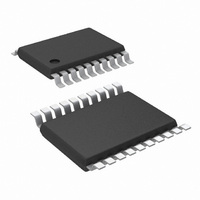
LM26420XMH/NOPB National Semiconductor, LM26420XMH/NOPB Datasheet - Page 19

LM26420XMH/NOPB
Manufacturer Part Number
LM26420XMH/NOPB
Description
IC REG SYNC BUCK DL 2A 20-TSSOP
Manufacturer
National Semiconductor
Series
PowerWise®r
Type
Step-Down (Buck)r
Datasheet
1.LM26420XSQNOPB.pdf
(28 pages)
Specifications of LM26420XMH/NOPB
Internal Switch(s)
Yes
Synchronous Rectifier
Yes
Number Of Outputs
2
Voltage - Output
0.8 ~ 4.5 V
Current - Output
2A
Frequency - Switching
2.2MHz
Voltage - Input
3 ~ 5.5 V
Operating Temperature
-40°C ~ 125°C
Mounting Type
Surface Mount
Package / Case
20-TSSOP Exposed Pad, 20-eTSSOP, 20-HTSSOP
Primary Input Voltage
5.5V
No. Of Outputs
2
Output Voltage
4.5V
Output Current
2A
No. Of Pins
20
Operating Temperature Range
-40°C To +125°C
Msl
MSL 1 - Unlimited
Filter Terminals
SMD
Rohs Compliant
Yes
Lead Free Status / RoHS Status
Lead free / RoHS Compliant
Power - Output
-
Other names
LM26420XMH
Thermal Definitions
T
T
R
R
Heat in the LM26420 due to internal power dissipation is re-
moved through conduction and/or convection.
Conduction: Heat transfer occurs through cross sectional ar-
eas of material. Depending on the material, the transfer of
heat can be considered to have poor to good thermal con-
ductivity properties (insulator vs. conductor).
Heat Transfer goes as:
Silicon
Convection: Heat transfer is by means of airflow. This could
be from a fan or natural convection. Natural convection occurs
when air currents rise from the hot device to cooler air.
Thermal impedance is defined as:
Thermal impedance from the silicon junction to the ambient
air is defined as:
The PCB size, weight of copper used to route traces and
ground plane, and number of layers within the PCB can great-
ly effect R
make a large difference in the thermal impedance. Thermal
vias are necessary in most applications. They conduct heat
from the surface of the PCB to the ground plane. Five to eight
thermal vias should be placed under the exposed pad to the
ground plane if the LLP package is used. Up to 12 thermal
vias should be used in the eTSSOP-20 package for optimum
heat transfer from the device to the ground plane.
Thermal impedance also depends on the thermal properties
of the application's operating conditions (V
and the surrounding circuitry.
Method 1: Silicon Junction Temperature Determination
To accurately measure the silicon temperature for a given
application, two methods can be used. The first method re-
quires the user to know the thermal impedance of the silicon
junction to top case temperature.
Some clarification needs to be made before we go any further.
R
package to silicon junction.
R
junction.
In this data sheet we will use R
to measure top case temperature with a small thermocouple
attached to the top case.
R
with the exposed pad. Knowing the internal dissipation from
the efficiency calculation given previously, and the case tem-
perature, which can be empirically measured on the bench
we have:
J
A
θJC
θJA
θJC
ΦJC
ΦJC
= Chip junction temperature
= Ambient temperature
= Thermal resistance from chip junction to ambient air
= Thermal resistance from chip junction to device case
is the thermal impedance from all six sides of an IC
is approximately 20°C/Watt for the 16-pin LLP package
is the thermal impedance from top case to the silicon
→
package
θJA
. The type and number of thermal vias can also
→
lead frame
ΦJC
→
PCB
so that it allows the user
IN
, V
OUT
, I
OUT
etc),
19
Therefore:
From the previous example:
Method 2: Thermal Shutdown Temperature Determina-
tion
The second method, although more complicated, can give a
very accurate silicon junction temperature.
The first step is to determine R
LM26420 has over-temperature protection circuitry. When the
silicon temperature reaches 165°C, the device stops switch-
ing. The protection circuitry has a hysteresis of about 15°C.
Once the silicon temperature has decreased to approximately
150°C, the device will start to switch again. Knowing this, the
R
stages of the design one may calculate the R
the PCB circuit into a thermal chamber. Raise the ambient
temperature in the given working application until the circuit
enters thermal shutdown. If the SW-pin is monitored, it will be
obvious when the internal FETs stop switching, indicating a
junction temperature of 165°C. Knowing the internal power
dissipation from the above methods, the junction tempera-
ture, and the ambient temperature R
Once this is determined, the maximum ambient temperature
allowed for a desired junction temperature can be found.
An example of calculating R
National Semiconductor LM26420 LLP demonstration board
is shown below.
The four layer PCB is constructed using FR4 with 1 oz copper
traces. The copper ground plane is on the bottom layer. The
ground plane is accessed by eight vias. The board measures
3.0cm x 3.0cm. It was placed in an oven with no forced airflow.
The ambient temperature was raised to 152°C, and at that
temperature, the device went into thermal shutdown.
From the previous example:
If the junction temperature was to be kept below 125°C, then
the ambient temperature could not go above 112°C.
θJA
for any application can be characterized during the early
125°C - (42.8°C/W x 304mW) = 112.0°C
T
T
T
j
j
j
= (R
= 20°C/W x 0.304W + T
- (R
P
INTERNAL
ΦJC
θJA
x P
x P
θJA
INTERNAL
INTERNAL
= 304mW
for an application using the
θJA
θJA
of the application. The
) = T
) + T
can be determined.
A
C
C
θJA
www.national.com
by placing


