ISL6529CBZ Intersil, ISL6529CBZ Datasheet
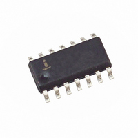
IC CTRLR/PWM BUCK SYNC 14SOIC

ISL6529CBZ

Manufacturer Part Number
ISL6529CBZ
Description
IC CTRLR/PWM BUCK SYNC 14SOIC
Manufacturer
Intersil
Type
Step-Down (Buck)r
Datasheet

Specifications of ISL6529CBZ

Internal Switch(s)
No
Synchronous Rectifier
Yes
Number Of Outputs
2
Voltage - Output
0.5 ~ 4.5 V
Frequency - Switching
600kHz
Operating Temperature
0°C ~ 70°C
Mounting Type
Surface Mount
Package / Case
14-SOIC (3.9mm Width), 14-SOL
Lead Free Status / RoHS Status
Lead free / RoHS Compliant
Current - Output
-
Voltage - Input
-
Power - Output
-

Available stocks

Company
Part Number
Manufacturer
Quantity
Price
Part Number:
ISL6529CBZ
Manufacturer:
INTERS
Quantity:
20 000
Part Number:
ISL6529CBZ-T
Manufacturer:
INTERSIL
Quantity:
20 000
Company:
Part Number:
ISL6529CBZ-T
Quantity:
500
Dual Regulator–Synchronous Rectified
Buck PWM and Linear Power Controllers
The ISL6529, ISL6529A provide the power control and
protection for two output voltages in high-performance
graphics cards and other embedded processor applications.
The dual-output controllers drive two N-Channel MOSFETs
in a synchronous rectified buck converter topology and one
N-Channel MOSFET in a linear configuration. The ISL6529,
ISL6529A provide both a regulated high current, low voltage
supply and an independent, lower current supply integrated
in a 14-lead SOIC package. The controllers are ideal for
graphic card applications where regulation of both the
graphics processing unit (GPU) and memory supplies is
required.
The synchronous rectified buck converters incorporate
simple, single feedback loop, voltage-mode control with fast
transient response. Both the switching regulator and linear
regulator provide a maximum static regulation tolerance of
±
user-adjustable by means of external resistors.
An integrated soft-start feature brings both supplies into
regulation in a controlled manner. Each output is monitored
via the FB pins for undervoltage events. If either output
drops below 51.5% of the nominal output level, both
converters are shut down.
Ordering Information
*Add “-T” suffix for tape and reel.
NOTE: Intersil Pb-free products employ special Pb-free material sets;
molding compounds/die attach materials and 100% matte tin plate
termination finish, which are RoHS compliant and compatible with both
SnPb and Pb-free soldering operations. Intersil Pb-free products are
MSL classified at Pb-free peak reflow temperatures that meet or
exceed the Pb-free requirements of IPC/JEDEC J STD-020.
ISL6529ACB
ISL6529ACBZ (Note)
ISL6529ACR
ISL6529ACRZ (Note)
ISL6529CB
ISL6529CBZ (Note)
ISL6529CR
ISL6529CRZ (Note)
ISL6529EVAL1
2% over line, load, and temperature ranges. Each output is
PART NUMBER*
RANGE (°C)
Evaluation Board
TEMP.
0 to 70
0 to 70
0 to 70
0 to 70
0 to 70
0 to 70
0 to 70
0 to 70
®
1
14 Ld SOIC
14 Ld SOIC (Pb-free) M14.15
16 Ld 5x5 QFN
16 Ld 5x5 QFN
(Pb-free)
14 Ld SOIC
14 Ld SOIC (Pb-free) M14.15
16 Ld 5x5 QFN
16 Ld 5x5 QFN
(Pb-free)
Data Sheet
PACKAGE
M14.15
L16.5x5B
L16.5x5B
M14.15
L16.5x5B
L16.5x5B
DWG. #
PKG.
CAUTION: These devices are sensitive to electrostatic discharge; follow proper IC Handling Procedures.
1-888-INTERSIL or 321-724-7143
Features
• Provides two regulated voltages
• Both controllers drive low cost N-Channel MOSFETs
• 12V direct drive saves external components
• Small converter size
• Excellent output voltage regulation
• 5V down conversion
• PWM and linear output voltage range: down to 0.8V
• Simple single-loop voltage-mode PWM control design
• Fast PWM converter transient response
• Linear controller drives N-Channel MOSFET pass transistor
• Fully-adjustable outputs
• Undervoltage fault monitoring on both outputs
• QFN Package:
• Pb-Free Available (RoHS Compliant)
Applications
• Graphics–GPU and memory supplies
• ASIC power supplies
• Embedded processor and I/O supplies
• DSP supplies
Related Literature
• Technical Brief TB363 Guidelines for Handling and
- One synchronous rectified buck PWM controller
- One linear controller
- 600kHz constant frequency operation
- Small external component count
- Both outputs: ±1% over temperature - ISL6529AC
- Both outputs: ±2% over temperature - ISL6529C
- High-bandwidth error amplifier
- Full 0-100% duty ratio
- Compliant to JEDEC PUB95 MO-220
- Near Chip Scale Package footprint, which improves
Processing Moisture Sensitive Surface Mount Devices
(SMDs)
QFN - Quad Flat No Leads - Package Outline
PCB efficiency and has a thinner profile
All other trademarks mentioned are the property of their respective owners.
April 12, 2005
Copyright © Intersil Americas Inc. 2002-2005. All Rights Reserved
|
Intersil (and design) is a trademark of Intersil Americas Inc.
ISL6529, ISL6529A
FN9070.5

Related parts for ISL6529CBZ

ISL6529CBZ Summary of contents

Page 1

... ISL6529ACBZ (Note SOIC (Pb-free) M14.15 ISL6529ACR 5x5 QFN ISL6529ACRZ (Note 5x5 QFN (Pb-free) ISL6529CB SOIC ISL6529CBZ (Note SOIC (Pb-free) M14.15 ISL6529CR 5x5 QFN ISL6529CRZ (Note 5x5 QFN (Pb-free) ISL6529EVAL1 Evaluation Board *Add “-T” suffix for tape and reel. NOTE: Intersil Pb-free products employ special Pb-free material sets; ...

Page 2

Pinouts ISL6529, ISL6529A (SOIC) TOP VIEW 1 LGATE PGND 2 3 GND 5VCC 4 5 DRIVE2 FB2 INTERNAL CONNECTION 2 ISL6529, ISL6529A 14 UGATE 13 12VCC COMP 9 FB ...

Page 3

Block Diagram VOLTAGE REFERENCE FB2 12VCC DRIVE2 EA2 INHIBIT SOFT-START GND 5VCC SHUTDOWN RESTART SOFT- START AND FAULT LOGIC INHIBIT SOFT-START +5VCC EA1 COMP1 OSCILLATOR UV1 UV2 FB COMP POWER-ON RESET (POR) 12VCC +5V UGATE GATE LOGIC PWM LGATE PGND ...

Page 4

Simplified Power System Diagram +V IN +12V +5V V OUT2 + Typical Application +V IN (+5V or +3.3V OUT2 2. OUT2 4 ISL6529, ISL6529A LINEAR Q3 CONTROLLER CONTROLLER ISL6529 ISL6529A + 5VCC ...

Page 5

Absolute Maximum Ratings UGATE, LGATE, DRIVE2 GND - 0.3V to 12VCC 5VCC . . . . . . . . . . . . . . ...

Page 6

Electrical Specifications Recommended Operating Conditions, Unless Otherwise Noted. Refer to Block and Simplified Power System Diagrams, and Typical Application Schematic (Continued) PARAMETER COMP Low Output, Sink Current Undervoltage Level ( REF PWM CONTROLLER GATE DRIVERS UGATE and ...

Page 7

FB2 (Pin 6), (Pin 5 QFN) Connect the output of the linear regulator to this pin through a properly sized resistor divider. The voltage at this pin is regulated to 0.8V. This pin is also monitored for undervoltage events. Pulling ...

Page 8

CAPACITOR CURRENT CAPACITOR CURRENT FIGURE 2. TOP SCOPE TRACES ARE VOLTAGE RAMP AND CAPACITOR CURRENT. LOWER TRACES ARE TIME AND VOLTAGE EXPANSION OF UPPER SCOPE TRACES. Undervoltage Protection The FB and FB2 pins are monitored during converter operation by two ...

Page 9

UGATE Q1 L OUT V OUT1 + LGATE C Q2 OUT1 FIGURE 4. OUTPUT VOLTAGE SELECTION OF THE PWM However, since the value of R1 affects the values of the rest of ...

Page 10

OSC DRIVER PWM COMP - + ∆ V OSC E/A V REF ERROR AMP DETAILED COMPENSATION COMPONENTS COMP ISL6529 0.8V FIGURE 6. VOLTAGE-MODE BUCK CONVERTER COMPENSATION DESIGN ...

Page 11

100   20 log -------- -   R1 -20 MODULATOR GAIN - ESR -60 10 100 1K 10K 100K FREQUENCY (Hz) FIGURE ...

Page 12

BODE PLOT OF REGULATOR (N0 COMP OUTPUT CURRENTS 0 3A -50 55mA -100 1mA -150 -200 1K 10 100 10K FREQUENCY (Hz) FIGURE 10. LOOP RESPONSE WITH ONLY 100µF, 5mΩ ...

Page 13

Figure 13 shows the results of the complete system with output capacitor and compensation network for 45° of phase margin. Because of the large variety of capacitors, varying ESRs and PC board layouts, Table 1, ...

Page 14

The final test for a system is transient load current performance. Ringing or oscillation indicates that the compensation network must be adjusted to assure stable operation with component and environmental variations. Figures 14 and 15 are scope shots that show ...

Page 15

VCC 5VCC C BP GND +12 VCC 12VCC C BP PGND Q1 UGATE PHASE ISL6529 Q2 LGATE COMP +3.3 V DRIVE2 R5 FB2 R6 KEY ...

Page 16

During this interval the difference between the inductor current and the load current must be supplied by the output capacitor(s). Minimizing the response ...

Page 17

... FIGURE 17. POWER SUPPLY APPLICATION CIRCUIT FOR A GRAPHICS CONTROLLER 17 ISL6529, ISL6529A The power dissipated in the linear regulator is: P LINEAR where I nominal output voltage of the linear regulator. References Intersil documents are available on the web at http://www.intersil.com. [1] Technical Brief, Intersil Corporation, TB417, http://www.intersil.com/data/tb/tb417.pdf L2 1µH +12V +5V C15 C5 1µ ...

Page 18

... Dimensions D2 and E2 are for the exposed pads which provide improved electrical and thermal performance. 8. Nominal dimensions are provided to assist with PCB Land Pattern Design efforts, see Intersil Technical Brief TB389. 9. Features and dimensions A2, A3, D1, E1, P & θ are present when Anvil singulation method is used and not present for saw singulation ...

Page 19

... Accordingly, the reader is cautioned to verify that data sheets are current before placing orders. Information furnished by Intersil is believed to be accurate and reliable. However, no responsibility is assumed by Intersil or its subsidiaries for its use; nor for any infringements of patents or other rights of third parties which may result from its use ...

Related keywords