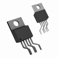
LM2585T-ADJ/NOPB National Semiconductor, LM2585T-ADJ/NOPB Datasheet - Page 11

LM2585T-ADJ/NOPB
Manufacturer Part Number
LM2585T-ADJ/NOPB
Description
IC MULTI CONFIG ADJ 3A TO220-5
Manufacturer
National Semiconductor
Series
SIMPLE SWITCHER®r
Type
Step-Up (Boost), Flyback, Forward Converterr
Datasheet
1.LM2585T-ADJNOPB.pdf
(28 pages)
Specifications of LM2585T-ADJ/NOPB
Internal Switch(s)
Yes
Synchronous Rectifier
No
Number Of Outputs
1
Voltage - Output
Adjustable
Current - Output
3A
Frequency - Switching
100kHz
Voltage - Input
4 ~ 40 V
Operating Temperature
-40°C ~ 125°C
Mounting Type
Through Hole
Package / Case
TO-220-5 (Bent and Staggered Leads)
Package
5TO-220
Minimum Input Voltage
4 V
Maximum Input Voltage
40 V
Switching Frequency
85 to 115 KHz
Operating Supply Voltage
4 to 40 V
Maximum Output Current
3 A
Output Type
Adjustable
Output Voltage
11.52 to 12.48 V
Efficiency
93(Typ) %
Dc To Dc Converter Type
Step Up
Pin Count
5 +Tab
Input Voltage
40V
Switching Freq
85 TO 115KHz
Output Current
3A
Package Type
TO-220
Switching Regulator
Yes
Load Regulation
100mV
Line Regulation
100mV
Mounting
Through Hole
Input Voltage (min)
4V
Operating Temperature Classification
Automotive
Primary Input Voltage
40V
No. Of Outputs
1
No. Of Pins
5
Operating Temperature Range
-40°C To +125°C
Msl
MSL 1 - Unlimited
Filter Terminals
Through Hole
Rohs Compliant
Yes
For Use With
551011367-061 - BOARD WEBENCH LM2577,LM2585/87
Lead Free Status / RoHS Status
Lead free / RoHS Compliant
Power - Output
-
Lead Free Status / Rohs Status
Compliant
Other names
*LM2585T-ADJ
*LM2585T-ADJ/NOPB
LM2585T-ADJ
*LM2585T-ADJ/NOPB
LM2585T-ADJ
Flyback Regulator Operation
The LM2585 is ideally suited for use in the flyback regulator
topology. The flyback regulator can produce a single output
voltage, such as the one shown in
voltages. In
put voltage that is inside the range of the input voltage. This
feature is unique to flyback regulators and cannot be dupli-
cated with buck or boost regulators.
The operation of a flyback regulator is as follows (refer to
Figure
primary winding of the transformer, T1, storing energy in the
magnetic field of the transformer. Note that the primary and
secondary windings are out of phase, so no current flows
through the secondary when current flows through the prima-
As shown in
regulator are shown in
4): when the switch is on, current flows through the
Figure
Figure
4, the LM2585 can be used as a flyback regulator by using a minimum number of external components. The switching waveforms of this
Figure
4, the flyback regulator generates an out-
5. Typical Performance Characteristics observed during the operation of this circuit are shown in
Figure
FIGURE 4. 12V Flyback Regulator Design Example
4, or multiple output
11
ry. When the switch turns off, the magnetic field collapses,
reversing the voltage polarity of the primary and secondary
windings. Now rectifier D1 is forward biased and current flows
through it, releasing the energy stored in the transformer. This
produces voltage at the output.
The output voltage is controlled by modulating the peak
switch current. This is done by feeding back a portion of the
output voltage to the error amp, which amplifies the difference
between the feedback voltage and a 1.230V reference. The
error amp output voltage is compared to a ramp voltage pro-
portional to the switch current (i.e., inductor current during the
switch on time). The comparator terminates the switch on time
when the two voltages are equal, thereby controlling the peak
switch current to maintain a constant output voltage.
1251521
Figure
6.
www.national.com


