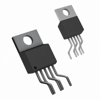
LM2585T-ADJ/NOPB National Semiconductor, LM2585T-ADJ/NOPB Datasheet - Page 18

LM2585T-ADJ/NOPB
Manufacturer Part Number
LM2585T-ADJ/NOPB
Description
IC MULTI CONFIG ADJ 3A TO220-5
Manufacturer
National Semiconductor
Series
SIMPLE SWITCHER®r
Type
Step-Up (Boost), Flyback, Forward Converterr
Datasheet
1.LM2585T-ADJNOPB.pdf
(28 pages)
Specifications of LM2585T-ADJ/NOPB
Internal Switch(s)
Yes
Synchronous Rectifier
No
Number Of Outputs
1
Voltage - Output
Adjustable
Current - Output
3A
Frequency - Switching
100kHz
Voltage - Input
4 ~ 40 V
Operating Temperature
-40°C ~ 125°C
Mounting Type
Through Hole
Package / Case
TO-220-5 (Bent and Staggered Leads)
Package
5TO-220
Minimum Input Voltage
4 V
Maximum Input Voltage
40 V
Switching Frequency
85 to 115 KHz
Operating Supply Voltage
4 to 40 V
Maximum Output Current
3 A
Output Type
Adjustable
Output Voltage
11.52 to 12.48 V
Efficiency
93(Typ) %
Dc To Dc Converter Type
Step Up
Pin Count
5 +Tab
Input Voltage
40V
Switching Freq
85 TO 115KHz
Output Current
3A
Package Type
TO-220
Switching Regulator
Yes
Load Regulation
100mV
Line Regulation
100mV
Mounting
Through Hole
Input Voltage (min)
4V
Operating Temperature Classification
Automotive
Primary Input Voltage
40V
No. Of Outputs
1
No. Of Pins
5
Operating Temperature Range
-40°C To +125°C
Msl
MSL 1 - Unlimited
Filter Terminals
Through Hole
Rohs Compliant
Yes
For Use With
551011367-061 - BOARD WEBENCH LM2577,LM2585/87
Lead Free Status / RoHS Status
Lead free / RoHS Compliant
Power - Output
-
Lead Free Status / Rohs Status
Compliant
Other names
*LM2585T-ADJ
*LM2585T-ADJ/NOPB
LM2585T-ADJ
*LM2585T-ADJ/NOPB
LM2585T-ADJ
www.national.com
FIGURE 23. Pulse PE-68413
FIGURE 24. Renco RL-5751
FIGURE 25. Renco RL-5533
FIGURE 26. Renco RL-5532
(Surface Mount)
Top View
Top View
Top View
Top View
T5
T7
T6
T5
1251543
1251540
1251542
1251539
18
Step-Up (Boost) Regulator
Operation
Figure 30
ulator. This is a switching regulator that produces an output
voltage greater than the input supply voltage.
A brief explanation of how the LM2585 Boost Regulator works
is as follows (refer to
on, the inductor current ramps up at the rate of V
energy in the inductor. When the switch turns off, the lower
end of the inductor flies above V
through diode (D) into the output capacitor (C
(V
switch on time is transferred to the output during the switch
off time. The output voltage is controlled by adjusting the peak
switch current, as described in the flyback regulator section.
OUT
− V
IN
shows the LM2585 used as a step-up (boost) reg-
)/L. Thus, energy stored in the inductor during the
FIGURE 28. Schott 67140900
FIGURE 29. Schott 67140890
FIGURE 27. Top View
Figure
Schott 26606
Top View
Top View
30). When the NPN switch turns
T7
T6
T5
IN
, discharging its current
OUT
1251546
) at a rate of
IN
1251547
/L, storing
1251544


