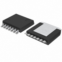
BD9778HFP-TR Rohm Semiconductor, BD9778HFP-TR Datasheet

BD9778HFP-TR
Specifications of BD9778HFP-TR
Available stocks
Related parts for BD9778HFP-TR
BD9778HFP-TR Summary of contents
Page 1
... Built-in overcurrent protection circuit 14) Built-in thermal shutdown protection circuit 15) High power HRP7 package mounted (BD9778HFP and BD9781HFP) Compact SOP8 package mounted (BD9778F and BD9001F) Applications All fields of industrial equipment, such as Flat TV , printer, DVD, car audio, car navigation, and communication such as ETC, AV, and OA. ...
Page 2
Absolute Maximum Ratings(Ta = 25˚C) Parameter Power supply BD9778F/HFP,BD9781HFP voltage BD9001F Output switch pin voltage BD9778F/HFP, BD9001F Output switch current BD9781HFP EN/SYNC, EN pin voltage RT, FB, INV pin voltage HRP7 Power dissipation SOP8 Operating temperature BD9778F/HFP,BD9781HFP range BD9001F Storage ...
Page 3
BD9001F (Unless otherwise specified, Ta=-40˚C ~ +95˚C,V Parameter Standby circuit current Circuit current [SW block] POWER MOS FET ON resistance Operating output current of overcurrent protection [Error Amp block] Reference voltage 1 Reference voltage 2 Reference voltage input regulation Input ...
Page 4
Reference data 1.020 1.015 1.010 1.005 1.000 0.995 0.990 0.985 0.980 -50 - 100 AMBIENT TEMPERATURE : Ta[ ] Fig.1 Output reference voltage vs. Ambient temprature (All series ...
Page 5
Ta=125 0.6 Ta=25 Ta=-40 0.4 0.2 0.0 0.0 0.5 1.0 1.5 2.0 2.5 OUTPUT CURRENT : I [A] O Fig.13 ON resistance V =7V IN (BD9778F/HFP) 1.8 1.6 1.4 1.2 Ta=125 1.0 0.8 Ta=25 ...
Page 6
... SW Output 2 N.C. Non Connection 3 FB Error Amp Output 4 INV Output voltage feedback 5 EN Enable 6 RT Frequency setting resistor connection 7 GND Ground 8 V Power supply input IN (BD9778HFP) EN ON/OFF 5 L:OFF H:ON 33μH DRIVER TSD 330μ CURRENT LIMIT 7 GND V FB INV EN IN ...
Page 7
Description of operations ERROR AMP The ERROR AMP block is an error amplifier used to input the reference voltage (1 V typ.) and the INV pin voltage. The output FB pin controls the switching duty and output voltage Vo. These ...
Page 8
Timing chart (BD9781HFP) - While in basic operation mode V IN Internal OSC FB SW EN/SYNC - While in overcurrent protection mode I O Internal OSC SW External synchronizing function (BD9781HFP) In order to activate the external synchronizing function, connect ...
Page 9
Description of external components Design procedure Vo = Output voltage, Vin (Max.) = Maximum input voltage Io (Max.) = Maximum load current Oscillation frequency 1. Setting or output voltage Output voltage can be ...
Page 10
... The set values listed above are all reference values. On the actual mounting of the IC, the characteristics may vary with the routing of wirings and the types of parts in use. In this connection recommended to thoroughly verify these values on the actual system prior to use. Directions for pattern layout of PCB 1 GND BD9778HFP R3 Cx1 C3 2 ...
Page 11
Cx2 R2 Fig.32 BD9001F reference layout pattern ※ As shown above, design the GND pattern as large area as possible within inner layer. ※ Gray zones indicate GND. 500 450 400 350 300 250 200 ...
Page 12
For output capacitors having high ESR, such as electrolyte capacitor For output capacitors that have high ESR (i.e., several Ω), the phase compensation setting procedure becomes comparatively simple. Since the DC/DC converter application has a LC resonant circuit attached ...
Page 13
Measurement of open loop of DC/DC converter To measure the open loop of DC/DC converter, use the gain phase analyzer or FRA to measure the frequency characteristics. DC/DC converter controller + Maximum load Load 0 Output voltage Heat loss ...
Page 14
SW RT VIN VIN SW 10kΩ RT EN(BD9778F/HFP, BD9001F) FB(BD9001F) VIN EN 300kΩ 250kΩ Cautions on use 1) Absolute maximum ratings An excess in the absolute maximum ratings, such as supply voltage, temperature range of operating conditions, etc., can break ...
Page 15
Ground wiring pattern It is recommended to separate the large-current GND pattern from the small-signal GND pattern and establish a single ground at the reference point of the set PCB, so that resistance to the wiring pattern and voltage ...
Page 16
Selection of order type ROHM model Product No. name 9778 = 36V/2A 9781 = 36V/4A 9001 = 50V/2A SOP8 <Outline dimensions> 5.0±0 0.1 1.27 0.4±0.1 HRP7 <Outline dimensions> 9.395 ± ...
Page 17
Appendix No technical content pages of this document may be reproduced in any form or transmitted by any means without prior permission of ROHM CO.,LTD. The contents described herein are subject to change without notice. The specifications for the product ...


