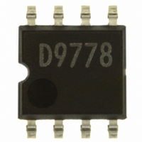
BD9778F-E2 Rohm Semiconductor, BD9778F-E2 Datasheet

BD9778F-E2
Specifications of BD9778F-E2
Available stocks
Related parts for BD9778F-E2
BD9778F-E2 Summary of contents
Page 1
... Furthermore, an external synchronization input pin (BD9781HFP) enables synchronous operation with external clock. Features 1) Minimal external components 2) Wide input voltage range (BD9778F/HFP and BD9781HFP (BD9001F) 3) Built-in P-ch POWER MOS FET 4) Output voltage setting enabled with external resistor Reference voltage accuracy: ±2% 6) Wide operating temperature range: -40˚ ...
Page 2
... Output voltage (ON Duty) Oscillation frequency Oscillation frequency set resistance Possible operating range Parameter Operating power supply voltage Electrical characteristics BD9778F/HFP (Unless otherwise specified -40˚C to +125˚C, V Parameter Standby circuit current Circuit current [SW block] POWER MOS FET ON resistance Operating output current of overcurrent protection ...
Page 3
BD9001F (Unless otherwise specified, Ta=-40˚C ~ +95˚C,V Parameter Standby circuit current Circuit current [SW block] POWER MOS FET ON resistance Operating output current of overcurrent protection [Error Amp block] Reference voltage 1 Reference voltage 2 Reference voltage input regulation Input ...
Page 4
... Fig.9 ON resistance V IN 1.8 1.6 1.4 1.2 Ta=125 1.0 Ta=25 0.8 Ta=125 Ta=-40 0.6 0.4 0.2 0.0 0.0 0.5 1.0 1.5 OUTPUT CURRENT : I Fig.12 ON resistance V (BD9781HFP) IN 125 25 - [V] IN (BD9781HFP) From the top, -40 25 125 [V] IN (BD9781HFP) 4.5 [A] O =5V (BD9781HFP) 2.0 2.5 [A] O =5V (BD9778F/HFP) ...
Page 5
... OUTPUT CURRENT : I [A] O Fig.15 ON resistance V =7V IN (BD9001F) 100 5V output 3.3V output 2.5V output 1.5V output 0.5 1.0 1.5 2.0 OUTPUT CURRENT : I [A] O Fig. Efficiency(V =12V,f=100kHz (BD9778F/HFP) 6 Ta=25 Ta=- Ta=125 OUTPUT CURRENT : I [A] O Fig.21 Current capacitance(V =12V,Vo=5V,f=100kHz) IN (BD9778F/HFP) ...
Page 6
... Block diagram / Application circuit / Pin assignment (BD9778F 220μF 1μF Vref SOFT START 23kΩ INV ERROR AMP PWM 4 - COMPARATOR - + LATCH + + 10kΩ 150kΩ RESET Vref GND EN 4700pF OSC PVIN RT SW INV 390kΩ 0.1μF Fig.23 No. Pin name Function ...
Page 7
... IC, this block will turn OFF the output to latch. The overcurrent protection detection values have been set as shown below: BD9781HFP . . . 8A(Typ.) BD9001F,BD9778F/HFP . . . 4A(Typ.) Furthermore, since this overcurrent protection is an automatically reset, after the output is turned OFF and latched, the latch will be reset with the RESET signal output by each oscillation frequency. ...
Page 8
Timing chart (BD9781HFP) - While in basic operation mode V IN Internal OSC FB SW EN/SYNC - While in overcurrent protection mode I O Internal OSC SW External synchronizing function (BD9781HFP) In order to activate the external synchronizing function, connect ...
Page 9
... Select the output capacitor having a value smaller than that obtained by the formula shown below. 3. -Io(Max)) Limit C = Max Vo I imit:2A(BD9778F/HFP,BD9001F), 4A(BD9781HFP this capacitance is not optimum, faulty startup may result. ( 3.5m is soft start time(min.)) INV ...
Page 10
Design procedure 4. Selection of diode Set diode rating with an adequate margin to the maximum load current. Also, make setting of the rated inverse voltage with an adequate margin to the maximum input voltage. A diode with a low ...
Page 11
... OSCILATING FREQUENCY SETTING RESISTANCE : R Fig. (BD9781HFP/BD9778F/HFP) T OSC ※Oscillation frequency s graph value is Typical value, oscillation frequency is necessary to consider Phase compensation setting procedure 1. Application stability conditions The following section describes the stability conditions of the negative feedback system. Since the DC/DC converter application is sampled according to the switching frequency, GBW (frequency at 0-dB gain) of the overall system should be set to 1/10 or less of the switching frequency ...
Page 12
For output capacitors having high ESR, such as electrolyte capacitor For output capacitors that have high ESR (i.e., several Ω), the phase compensation setting procedure becomes comparatively simple. Since the DC/DC converter application has a LC resonant circuit attached ...
Page 13
Measurement of open loop of DC/DC converter To measure the open loop of DC/DC converter, use the gain phase analyzer or FRA to measure the frequency characteristics. DC/DC converter controller + Maximum load Load 0 Output voltage Heat loss ...
Page 14
... Accordingly, methods by which parasitic diodes operate, such as applying a voltage that is lower than the GND (P substrate) voltage to an input pin, should not be used. Resistor (Pin layer Parasitic element GND Fig.37 Typical simple construction of monolithic IC FB(BD9778F/HFP, BD9781HFP) VREF 50kΩ VIN FB 300kΩ 2kΩ VREF VIN FB 1kΩ 1kΩ Fig.36 Equivalent circuit ...
Page 15
... SOP8 0.8 0.7 0.6 0.5 0.4 0.3 0.2 0.1 0 125 150 0 25 Single piece of IC When mounted on ROHM standard PCB (Glass epoxy PCB 1.6 mm 15/ bypass diode between each pin and V IN BD9778F BD9001F 50 75 100 125 AMBIENT TEMPERATURE Ta Fig. 150 ...
Page 16
Selection of order type ROHM model Product No. name 9778 = 36V/2A 9781 = 36V/4A 9001 = 50V/2A SOP8 <Outline dimensions> 5.0±0 0.1 1.27 0.4±0.1 HRP7 <Outline dimensions> 9.395 ± ...
Page 17
Appendix No technical content pages of this document may be reproduced in any form or transmitted by any means without prior permission of ROHM CO.,LTD. The contents described herein are subject to change without notice. The specifications for the product ...


