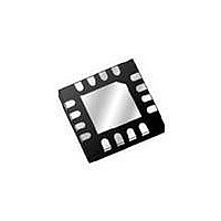
MAX15041ETE+ Maxim Integrated Products, MAX15041ETE+ Datasheet - Page 10

MAX15041ETE+
Manufacturer Part Number
MAX15041ETE+
Description
IC DCDC CONV STP-DN SYNC 16TQFN
Manufacturer
Maxim Integrated Products
Type
Step-Down (Buck)r
Datasheet
1.MAX15041ETE.pdf
(18 pages)
Specifications of MAX15041ETE+
Internal Switch(s)
Yes
Synchronous Rectifier
Yes
Number Of Outputs
1
Voltage - Output
0.6 ~ 25.2 V
Current - Output
3A
Frequency - Switching
350kHz
Voltage - Input
4.5 ~ 28 V
Operating Temperature
-40°C ~ 85°C
Mounting Type
Surface Mount
Package / Case
16-TQFN Exposed Pad
Power - Output
1.67W
Output Voltage
5.1 V
Supply Current
2.1 mA
Switching Frequency
350 KHz
Mounting Style
SMD/SMT
Maximum Operating Temperature
+ 85 C
Minimum Operating Temperature
- 40 C
Lead Free Status / RoHS Status
Lead free / RoHS Compliant
Low-Cost, 3A, 4.5V to 28V Input, 350kHz, PWM
Step-Down DC-DC Regulator with Internal Switches
The MAX15041 is a high-efficiency, peak-current-
mode, step-down DC-DC converter with integrated
high-side (170mΩ, typ) and low-side (105mΩ, typ)
power switches. The output voltage is set from 0.606V
to 0.9 x V
divider and can deliver up to 3A load current. The 4.5V
to 28V input voltage range makes the device ideal for
distributed power systems, notebook computers, and
preregulation applications.
The MAX15041 features a PWM, internally fixed 350kHz
switching frequency with a 90% maximum duty cycle.
PWM current-mode control allows for an all-ceramic
capacitor solution. The MAX15041 comes with a high-
gain transconductance error amplifier. The current-
mode control architecture simplifies compensation
design and ensures a cycle-by-cycle current limit and
fast reaction to line and load transients. The low
R
ciency at heavy loads and minimize critical induc-
tances, reducing layout sensitivity.
The MAX15041 also features thermal shutdown and
overcurrent protection (high-side sourcing and low-side
sinking), and an internal 5V, LDO with undervoltage
lockout. An externally adjustable voltage soft-start
gradually ramps up the output voltage and reduces
inrush current. Independent enable control and power-
good signals allow for flexible power sequencing. The
MAX15041 also provides the ability to start up into a
prebiased output, below or above the set point.
The MAX15041 operates at a constant 350kHz switch-
ing frequency. When EN is high, after a brief settling
time, PWM operation starts when V
voltage, at the beginning of soft-start.
The first operation is always a high-side MOSFET turn-
on, at the beginning of the clock cycle. The high-side
MOSFET is turned off when:
1) COMP voltage crosses the internal current-mode
10
DS-ON
ramp waveform, which is the sum of the compensa-
tion ramp and the current-mode ramp derived from
the inductor current waveform (current-sense block).
______________________________________________________________________________________
, on-chip, MOSFET switches ensure high effi-
IN
by using an adjustable, external resistive
Controller Function—PWM Logic
Detailed Description
SS
crosses the FB
2) The high-side MOSFET current limit is reached.
3) The maximum duty cycle of 90% is reached.
Then, the low-side MOSFET turns on; the low-side
MOSFET turns off when the clock period ends.
The MAX15041 is capable of safely soft-starting into a
prebiased output without discharging the output
capacitor. Starting up into a prebiased condition, both
low-side and high-side MOSFETs remain off to avoid
discharging the prebiased output. PWM operation
starts only when the SS voltage crosses the FB voltage.
The MAX15041 is also capable of soft-starting into an
output prebiased above the OUT nominal set point. In
this case, forced PWM operation starts when SS volt-
age reaches 0.65V (typ).
In case of a prebiased output, below or above the OUT
nominal set point, if the low-side MOSFET sink current
reaches the sink current limit (-3A, typ), the low-side
MOSFET turns off before the end of the clock period
and the high-side MOSFET turns on until one of the fol-
lowing conditions happens:
1) High-side MOSFET source current hits the reduced
2) The clock period ends.
The MAX15041 features independent device enable
control and power-good signals that allow for flexible
power sequencing. The enable input (EN) is an input
with a 1.95V (typ) threshold that controls the regulator.
Assert a voltage exceeding the threshold on EN to
enable the regulator, or connect EN to IN for always-on
operations. Power-good (PGOOD) is an open-drain
output that deasserts (goes high impedance) when V
is above 560mV (typ), and asserts low if V
545mV (typ).
When the EN voltage is higher than 1.4V (typ) and
lower than 1.95V (typ), most of the internal blocks are
disabled, only an internal coarse preregulator, includ-
ing the EN accurate comparator, is kept on.
high-side MOSFET current limit (0.75A, typ); in this
case, the high-side MOSFET is turned off for the
remaining clock period.
Enable Input and Power-Good Output
Starting into a Prebiased Output
FB
is below
FB


