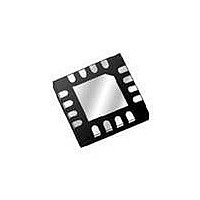
MAX15041ETE+ Maxim Integrated Products, MAX15041ETE+ Datasheet - Page 12

MAX15041ETE+
Manufacturer Part Number
MAX15041ETE+
Description
IC DCDC CONV STP-DN SYNC 16TQFN
Manufacturer
Maxim Integrated Products
Type
Step-Down (Buck)r
Datasheet
1.MAX15041ETE.pdf
(18 pages)
Specifications of MAX15041ETE+
Internal Switch(s)
Yes
Synchronous Rectifier
Yes
Number Of Outputs
1
Voltage - Output
0.6 ~ 25.2 V
Current - Output
3A
Frequency - Switching
350kHz
Voltage - Input
4.5 ~ 28 V
Operating Temperature
-40°C ~ 85°C
Mounting Type
Surface Mount
Package / Case
16-TQFN Exposed Pad
Power - Output
1.67W
Output Voltage
5.1 V
Supply Current
2.1 mA
Switching Frequency
350 KHz
Mounting Style
SMD/SMT
Maximum Operating Temperature
+ 85 C
Minimum Operating Temperature
- 40 C
Lead Free Status / RoHS Status
Lead free / RoHS Compliant
Low-Cost, 3A, 4.5V to 28V Input, 350kHz, PWM
Step-Down DC-DC Regulator with Internal Switches
A larger inductor value results in reduced inductor ripple
current, leading to a reduced output ripple voltage.
However, a larger inductor value results in either a larger
physical size or a higher series resistance (DCR) and a
lower saturation current rating. Typically, inductor value
is chosen to have current ripple equal to 30% of load
current. Choose the inductor with the following formula:
where f
quency, and ∆I
(typically set to 0.3 x I
inductor current, I
minimum high-side MOSFET current-limit value,
I
rating, I
satisfied:
The MAX15041 requires an external bootstrap steering
diode. Connect the diode between V
diode should have a reverse voltage rating, higher than
the converter input voltage and a 150mA minimum cur-
rent rating. Typically, a fast switching or Schottky diode
is used in this application, such as a 1N4148 diode.
For a step-down converter, input capacitor C
keep the DC input voltage steady, in spite of discontin-
uous input AC current. Low-ESR capacitors are pre-
ferred to minimize the voltage ripple due to ESR.
Size C
Low-ESR capacitors are recommended to minimize the
voltage ripple due to ESR. Total output-voltage peak-to-
peak ripple is estimated by the following formula:
12
HSCL_MIN
V
OUT
I
L PK
______________________________________________________________________________________
_
IN
SW
L_SAT
using the following formula:
f
SW
V
C
OUT
(5A, typ), and the inductor saturation current
is the internally fixed 350kHz switching fre-
I
LOAD
IN
. Ensure that the following relationship is
L
L
L
f
is the estimated inductor ripple current
SW
1
L_PK,
f
SW
1
2
Output-Capacitor Selection
V
V
OUT
V
OUT
IN
Input Capacitor Selection
I
LOAD
must always be below both the
V
I
LOAD
L
IN RIPPLE
I
L
_
min(
R
ESR COUT
). In addition, the peak
1
Inductor Selection
I
HSCL MIN L SAT
_
V
Diode Selection
OUT
V
IN
V
DD
_
OUT
V
IN
8 8 f
and BST. The
,
I
SW
IN
_
1
helps to
C
OUT
)
For ceramic capacitors, ESR contribution is negligible:
For tantalum or electrolytic capacitors, ESR contribution
is dominant:
The MAX15041 uses a fixed-frequency, peak-current-
mode control scheme to provide easy compensation
and fast transient response. The inductor peak current is
monitored on a cycle-by-cycle basis and compared to
the COMP voltage (output of the voltage error amplifier).
The regulator’s duty-cycle is modulated based on the
inductor’s peak current value. This cycle-by-cycle con-
trol of the inductor current emulates a controlled current
source. As a result, the inductor’s pole frequency is
shifted beyond the gain-bandwidth of the regulator.
System stability is provided with the addition of a sim-
ple series capacitor-resistor from COMP to SGND. This
pole-zero combination serves to tailor the desired
response of the closed-loop system.
The basic regulator loop consists of a power modulator
(comprising the regulator’s pulse-width modulator,
compensation ramp, control circuitry, MOSFETs, and
inductor), the capacitive output filter and load, an out-
put feedback divider, and a voltage-loop error amplifier
with its associated compensation circuitry. See Figure 1
for a graphical representation.
The average current through the inductor is expressed as:
where I
the power modulator’s transconductance. For a buck
converter:
where R
Combining the two previous equations, the power mod-
ulator’s transfer function in terms of V
to V
COMP
L
LOAD
V
is the average inductor current and G
is:
V
COMP
OUT
R
R
Compensation Design Guidelines
ESR COUT
ESR COUT
is the equivalent load resistor value.
_
_
I
V
L
R
OUT
LOAD
G
G
MOD
MOD
I
L
R
LOAD
8
8
I
L
V
f
f
COMP
SW
SW
R
LOAD
1
1
I
L
C
C
OUT
OUT
OUT
G
MOD
with respect
MOD
is


