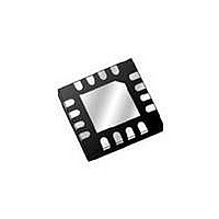
MAX15041ETE+ Maxim Integrated Products, MAX15041ETE+ Datasheet - Page 16

MAX15041ETE+
Manufacturer Part Number
MAX15041ETE+
Description
IC DCDC CONV STP-DN SYNC 16TQFN
Manufacturer
Maxim Integrated Products
Type
Step-Down (Buck)r
Datasheet
1.MAX15041ETE.pdf
(18 pages)
Specifications of MAX15041ETE+
Internal Switch(s)
Yes
Synchronous Rectifier
Yes
Number Of Outputs
1
Voltage - Output
0.6 ~ 25.2 V
Current - Output
3A
Frequency - Switching
350kHz
Voltage - Input
4.5 ~ 28 V
Operating Temperature
-40°C ~ 85°C
Mounting Type
Surface Mount
Package / Case
16-TQFN Exposed Pad
Power - Output
1.67W
Output Voltage
5.1 V
Supply Current
2.1 mA
Switching Frequency
350 KHz
Mounting Style
SMD/SMT
Maximum Operating Temperature
+ 85 C
Minimum Operating Temperature
- 40 C
Lead Free Status / RoHS Status
Lead free / RoHS Compliant
Low-Cost, 3A, 4.5V to 28V Input, 350kHz, PWM
Step-Down DC-DC Regulator with Internal Switches
2) Place capacitors on V
3) Keep the high-current paths as short and wide as
Figure 3. Typical Operating Circuit (4.5V to 28V Input Buck Converter)
Table 1. Typical Component Values for Common Output-Voltage Settings
16
possible to the IC and the corresponding pin using
direct traces. Keep the power ground plane (con-
nected to PGND) and signal ground plane (connect-
ed to SGND) separate. PGND and SGND connect at
only one common point near the input bypass
capacitor return terminal.
possible. Keep the path of switching current short
and minimize the loop area formed by LX, the output
capacitors, and the input capacitors.
4.5V TO 28V
______________________________________________________________________________________
V
INPUT
OUT
PGOOD
5.0
3.3
2.5
1.8
1.2
C
47 F
IN
(V)
10k
R
PU
L (µH)
DD
4.7
4.7
3.3
2.2
2.2
C
1 F
, IN, and SS as close as
VDD
C
0.01 F
SS
IN
EN
V
PGOOD
SS
DD
C
I.C.
C
MAX15041
12
22
33
47
8
(nF)
D
SGND
COMP
PGND
BST
LX
FB
100pF
4) Connect IN, LX, and PGND separately to a large
5) Ensure all feedback connections are short and
6) Route high-speed switching nodes (such as LX and
C
CC
R
47
copper area to help cool the IC to further improve
efficiency.
direct. Place the feedback resistors and compensa-
tion components as close as possible to the IC.
BST) away from sensitive analog areas (such as FB
and COMP).
BST
R
10nF
C
C
2.70
1.80
1.50
1.00
0.68
BST
(k )
R
1.8k
C
12nF
C
C
4.7 H
Calculate R
L
Setting the Output Voltage section.
22 F
C
OUT
Select R
5k
1
using the equation in the
R
1
and R
R
2
2
so that:
R
45.3k
1%
R
10.0k
1%
50k
1
2
2
OUTPUT = 3.3V


