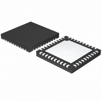
MAX8686ETL+ Maxim Integrated Products, MAX8686ETL+ Datasheet - Page 19

MAX8686ETL+
Manufacturer Part Number
MAX8686ETL+
Description
IC BUCK SYNC ADJ 25A 40TQFN
Manufacturer
Maxim Integrated Products
Type
Step-Down (Buck)r
Datasheet
1.MAX8686ETL.pdf
(23 pages)
Specifications of MAX8686ETL+
Internal Switch(s)
Yes
Synchronous Rectifier
Yes
Number Of Outputs
1
Voltage - Output
0.7 ~ 5.5 V
Current - Output
25A
Frequency - Switching
300kHz ~ 1MHz
Voltage - Input
4.5 ~ 20 V
Operating Temperature
-40°C ~ 85°C
Mounting Type
Surface Mount
Package / Case
40-TQFN Exposed Pad
Power - Output
4W
Lead Free Status / RoHS Status
Lead free / RoHS Compliant
ripple-current requirement (I
switching currents as defined by the following equations:
for (N x D) ≤ 1:
for (N x D) > 1.
where N is the number of phases, D is the duty cycle,
and I
Use the minimum input voltage for calculating the duty
cycle to obtain the worst-case input-capacitor RMS rip-
ple current. Low-ESR aluminum electrolytic, polymer, or
ceramic capacitors should be used to avoid large volt-
age transients at the input during a large step load
change at the output. The ripple-current specifications
provided by the manufacturer should be carefully
reviewed for temperature derating. Additional small-
value, low-ESL ceramic capacitors (1μF to 10μF with
proper voltage rating) can be used in parallel to reduce
any high-frequency ringing.
The minimum output capacitance, C
required to meet load-dump requirements. The worst-
case load dump is a sudden transition from full load
current (I
(I
balance from:
Figure 6. Compensation Components
2 OUT_MIN
DC-DC Converter Delivers Up to 25A Per Phase
I
OUT_MAX
RMS
C
OUT MIN
=
I
RMS
). C
2 OUT_MAX
D I
MAX8686
(
×
is the maximum output current.
OUT(MIN)
=
OUT MAX
)
D I
______________________________________________________________________________________
≥
×
_
N
L
OUT MAX
COMP
×
) to minimum load current
(
V
(
is estimated based on energy
I
FIN
2
OUT MAX
_
×
+
N D
_
V
3
×
×
OV
RMS
Output Capacitor
) )
N D
−
2
−
) imposed by the
R
×
(
1
I
−
C
N D
C
2
OUT MIN
C
V
×
INIT
2
−
_
1
OUT(MIN)
)
Single/Multiphase, Step-Down,
2
2
−
C
F
)
1
, is
where I
values of the load current during the worst-case load
dump, V
is the steady-state voltage after the load dump, and
V
term (V
output voltage reached during the load dump. The
above equation is an approximation, and the output
capacitance value obtained serves as a good starting
point. The final value should be obtained from actual
measurements. For ceramic output capacitors, the out-
put capacitor requirement is determined mostly by load
dump requirements due to their low ESR and ESL. See
Figures 7 and 8.
The MAX8686 uses an internal transconductance error
amplifier whose output compensates the control loop.
The external inductor, output capacitor, compensation
Figure 7. Simplified Gain Plot for the f zMOD > f C Case
Figure 8. Simplified Gain Plot for the f zMOD < f C Case
MODULATOR
OV
MODULATOR
POWER
is the allowed voltage overshoot above V
POWER
2 OUT_MAX
FIN
INIT 2
GAIN
(dB)
+ V
GAIN
(dB)
0
is the voltage prior to the load dump, V
0
OV
VOLTAGE-
DIVIDER
VOLTAGE-
DIVIDER
and I
) represents the maximum transient
fp
fp
2 OUT_MIN
CLOSED LOOP
MOD
MOD
CLOSED LOOP
Compensation Design
fz
MOD
f
C
fz
are the initial and final
MOD
f
C
ERROR
AMPLIFIER
ERROR
AMPLIFIER
FREQUENCY (Hz)
FREQUENCY (Hz)
FIN
. The
FIN
19


