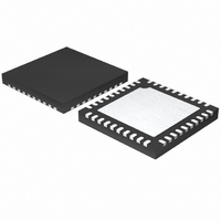
MAX8686ETL+ Maxim Integrated Products, MAX8686ETL+ Datasheet - Page 20

MAX8686ETL+
Manufacturer Part Number
MAX8686ETL+
Description
IC BUCK SYNC ADJ 25A 40TQFN
Manufacturer
Maxim Integrated Products
Type
Step-Down (Buck)r
Datasheet
1.MAX8686ETL.pdf
(23 pages)
Specifications of MAX8686ETL+
Internal Switch(s)
Yes
Synchronous Rectifier
Yes
Number Of Outputs
1
Voltage - Output
0.7 ~ 5.5 V
Current - Output
25A
Frequency - Switching
300kHz ~ 1MHz
Voltage - Input
4.5 ~ 20 V
Operating Temperature
-40°C ~ 85°C
Mounting Type
Surface Mount
Package / Case
40-TQFN Exposed Pad
Power - Output
4W
Lead Free Status / RoHS Status
Lead free / RoHS Compliant
Single/Multiphase, Step-Down,
DC-DC Converter Delivers Up to 25A Per Phase
resistor, and compensation capacitors determine the
loop stability. The inductor and output capacitor are
chosen based on performance, size, and cost.
Additionally, the compensation resistor and capacitors
are selected to optimize control-loop stability. The compo-
nent values, shown in Figures 2, 3, and 4, yield stable
operation over the given range of input-to-output voltages.
The regulator uses a current-mode control scheme that
regulates the output voltage by forcing the required
current through the external inductor. The voltage drop
across the DC resistance of the inductor or the alter-
nate series current-sense resistor is used to measure
the inductor current. Current-mode control eliminates
the double pole in the feedback loop caused by the
inductor and output capacitor resulting in a smaller
phase shift and requiring a less elaborate error-amplifi-
er compensation than voltage-mode control. A simple
series R
high-bandwidth loop in applications where ceramic
capacitors are used for output filtering. For other types
of capacitors, due to the higher capacitance and ESR,
the frequency of the zero created by the capacitance
and ESR is lower than the desired closed-loop crossover
frequency. To stabilize a nonceramic output-capacitor
loop, add another compensation capacitor from COMP
to GND to cancel this ESR zero. See Figure 6.
The basic regulator loop is modeled as a power modula-
tor, an output feedback divider, and an error amplifier.
The power modulator has DC gain set by g
with a pole and zero pair set by R
itor (C
Below are equations that define the power modulator:
where R
ing frequency, L is the output inductance, g
1/(A
sense amplifier (30.5 typ), R
the inductor, the duty cycle D = V
20
G
VCS
MOD DC
______________________________________________________________________________________
OUT
C
LOAD
x R
(
and C
), and its equivalent series resistance (ESR).
)
DC
=
= V
), where A
g
C
mc
OUT
is all that is needed to have a stable,
×
⎡
⎢
⎣
1
/[I
+
OUT(MAX)
R
L f
VCS
LOAD
×
SW
DC
is the gain of the current-
×
LOAD
is the DC resistance of
R
⎡
⎣
/N], f
OUT
(
LOAD
K
S
, the output capac-
/V
× −
SW
(
IN
1
. K
is the switch-
mc
D
S
)
)
is a slope
x R
−
0. . 5
LOAD
mc
⎤
⎦
⎤
⎥
⎦
=
,
compensation factor calculated from the following
equation:
Find the pole and zero frequencies created by the
power modulator as follows:
when C
lel, the resulting C
ESR
combination of like capacitors is the same as for an
individual capacitor.
The transconductance error amplifier has a DC gain,
G
er transconductance, which is equal to 1.7mS, and R
is the output resistance of the error amplifier, which is
30MΩ. A dominant pole (f
sation capacitor (C
(R
is set by the compensation resistor (R
pensation capacitor (C
(f
ESR zero if it occurs near the crossover frequency (f
Thus:
The crossover frequency, f
than the power-modulator pole f
pEA
EA(DC)
f
O
pMOD
), and the compensation resistor (R
(EACH)
) set by C
=
OUT
2
= g
π
×
/n. Note that the capacitor zero for a parallel
K
R
f
pdEA
comprises “n” identical capacitors in paral-
mEA
LOAD
S
f
zMOD
= +
N
F
f
f
zEA
pEA
1
and R
×
=
x R
C
OUT
2
V
OUT
=
f
=
C
=
π
OUT
SW
O
), the amplifier output resistance
2
2
×
2π
, where g
π
π
+
C
C
= n x C
x L x V
⎡
⎢
⎣
×
×
C
−
2
C
×
to cancel the output capacitor
π
C
). There is an optional pole
C C
pdEA
0 182
C
×
× ×
1
1
C
F
1
.
L f
C
OUT
(
R
×
×
, should be much higher
1
(
O
SW
R
R
N
) is set by the compen-
IN
mEA
OUT(EACH)
C
+
C
PMOD
×
x V
×
R
−
ESR
C
C
OUT
IN MIN
V V
is the error-amplifi-
)
OUT
_
. Also, f
C
×
C
) and the com-
[
); a zero (f
K
)
S
, and ESR =
× −
(
1
C
D
) )
−
should
0 5
.
zEA
]
C
⎤
⎥
⎦
O
).
)


