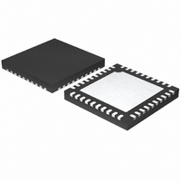
MAX8686ETL+ Maxim Integrated Products, MAX8686ETL+ Datasheet - Page 21

MAX8686ETL+
Manufacturer Part Number
MAX8686ETL+
Description
IC BUCK SYNC ADJ 25A 40TQFN
Manufacturer
Maxim Integrated Products
Type
Step-Down (Buck)r
Datasheet
1.MAX8686ETL.pdf
(23 pages)
Specifications of MAX8686ETL+
Internal Switch(s)
Yes
Synchronous Rectifier
Yes
Number Of Outputs
1
Voltage - Output
0.7 ~ 5.5 V
Current - Output
25A
Frequency - Switching
300kHz ~ 1MHz
Voltage - Input
4.5 ~ 20 V
Operating Temperature
-40°C ~ 85°C
Mounting Type
Surface Mount
Package / Case
40-TQFN Exposed Pad
Power - Output
4W
Lead Free Status / RoHS Status
Lead free / RoHS Compliant
be less than or equal to 1/5 the switching frequency.
Select a value for f
The feedback voltage-divider gain (V
be included for an output voltage higher than 3.3V,
where V
At the crossover frequency, the total loop gain must
equal 1, and is expressed as:
For the case where f
Then R
where g
The error-amplifier compensation zero formed by R
and C
Calculate the value of C
If f
from COMP to GND. The value of C
As the load current decreases, the modulator pole also
decreases; however, the modulator gain increases
accordingly and the crossover frequency remains the
same.
For the case where f
The power modulator gain at f
DC-DC Converter Delivers Up to 25A Per Phase
PMOD
C
C
REFIN
mEA
should be set at the modulator pole f
is less than 5 x f
can be calculated as:
G
G
G
= 1.7mS.
R
is equal to 3.3V.
MOD fc
MOD fc
EA fc
C
C
C
( )
=
G
C
F
______________________________________________________________________________________
C
( )
( )
g
EA fc
f
pMOD
mEA
×
=
zMOD
=
zMOD
in the range:
( )
G
2π
=
2π
=
MOD fc
C
G
G
×
=
×
×
C
MOD dc
MOD dc
<<
as follows:
V
is greater than f
is less than f
R
, add a second capacitor C
g
f
REFIN
pMOD
( )
mEA
C
V
f
C
1
OUT
1
C
( )
( )
×
×
≤
f
is:
zMOD
×
V
×
f
V
×
SW
×
×
REFIN
R
5
OUT
G
R
F
C
f
f
f
pMOD
pMOD
zMOD
MOD fc
C
is:
REF
f
C
C
= 1
:
( )
/V
C
Single/Multiphase, Step-Down,
OUT
:
) should
PMOD
C
F
.
The error-amplifier gain at f
R
where g
C
C
The current-mode control model on which the above
design procedure is based requires an additional high-
frequency term, G
pling the peak inductor current. The term G
additional phase lag at crossover and should be modeled
to estimate the phase margin obtainable by the selected
compensation components. As a final step, it is useful to
plot the dB gain and phase of the following loop-gain
transfer function and check the obtained phase margin. A
phase margin of at least 45° is recommended:
where the sampling effect quality factor is:
G
C
C
F
LOOP
is calculated from:
is calculated as:
is calculated from:
( )
s
mEA
R
=
(
1
C
⎡
⎢
⎣
G s
+
1
+
s
S
=
L f
/
= 1.7mS.
R
G
( ) =
2
LOAD
V
×
π
EA fc
V
OUT
Q
SW
×
FB
(
1
C
C
( )
R
f
C
pEA
+
⎛
⎜
⎜
⎝
C
F
S
LOAD
×
1
s
(s), to account for the effect of sam-
=
×
+
⎡ ⎣
/
=
) (
=
(
=
2
Ks
× +
[
g
π
π
π (
2π
2π
g
×
1
mEA
×
×
× −
mEA
×
g
f
(
zEA
Q
MC
1
s
×
×
K
/
c
R
C
s
f
2
D
S
pMOD
×
)
π
C
×
×
)
× −
is:
)
G
×
1
1
R
−
f
×
SW
(
MOD fc
f
1
pdEA
0 0 5
1
C
1
f
.
zMOD
f
×
C
⎤ ⎦
×
D
+
⎤
⎥
⎦
)
( )
)
R
f
×
(
zMOD
× ×
−
π
C
(
(
1
1
g
f
C
0 5
+
+
mEA
×
×
. )
s
s
s
f
SW
f
2
zMOD
/
/
2
2
]
×
S
π
V
π
Ro V
(s) produces
)
OUT
×
×
2
f
f
pMOD
×
zMOD
⎞
⎟
⎟
⎠
REFIN
)
)
× ×
G
21
S
(


