LM2596T-5.0/NOPB National Semiconductor, LM2596T-5.0/NOPB Datasheet - Page 13
LM2596T-5.0/NOPB
Manufacturer Part Number
LM2596T-5.0/NOPB
Description
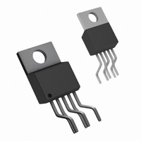
IC REG SIMPLE SWITCHER TO-220-5
Manufacturer
National Semiconductor
Series
SIMPLE SWITCHER®r
Type
Step-Down (Buck)r
Datasheet
1.LM2596S-ADJNOPB.pdf
(31 pages)
Specifications of LM2596T-5.0/NOPB
Internal Switch(s)
Yes
Synchronous Rectifier
No
Number Of Outputs
1
Voltage - Output
5V
Current - Output
3A
Frequency - Switching
150kHz
Voltage - Input
4.5 ~ 40 V
Operating Temperature
-40°C ~ 125°C
Mounting Type
Through Hole
Package / Case
TO-220-5 (Bent and Staggered Leads)
Primary Input Voltage
12V
No. Of Outputs
1
Output Voltage
5V
Output Current
3A
No. Of Pins
5
Operating Temperature Range
-40°C To +125°C
Filter Terminals
Through Hole
Rohs Compliant
Yes
For Use With
551011367-041 - BOARD WEBENCH BUILD IT
Lead Free Status / RoHS Status
Lead free / RoHS Compliant
Power - Output
-
Other names
*LM2596T-5.0
*LM2596T-5.0/NOPB
LM2596T-5.0
*LM2596T-5.0/NOPB
LM2596T-5.0
Available stocks
Company
Part Number
Manufacturer
Quantity
Price
Company:

Part Number:
LM2596T-5.0/NOPB
Manufacturer:
NS44
Quantity:
315
Part Number:
LM2596T-5.0/NOPB
Manufacturer:
TI/德州仪器
Quantity:
20 000


Given:
V
V
I
F = Switching Frequency (Fixed at a nominal 150 kHz).
1. Programming Output Voltage (Selecting R
shown in Figure 1 )
Use the following formula to select the appropriate resistor
values.
Select a value for R
resistor values minimize noise pickup in the sensitive feed-
back pin. (For the lowest temperature coefficient and the best
stability with time, use 1% metal film resistors.)
2. Inductor Selection (L1)
A. Calculate the inductor Volt • microsecond constant E • T (V
where V
and V
B. Use the E • T value from the previous formula and match it
with the E • T number on the vertical axis of the Inductor Value
Selection Guide shown in Figure 7 .
C. on the horizontal axis, select the maximum load current.
D. Identify the inductance region intersected by the E • T value
and the Maximum Load Current value. Each region is identi-
fied by an inductance value and an inductor code (LXX).
E. Select an appropriate inductor from the four manufacturer’s
part numbers listed in Figure 8 .
• µs), from the following formula:
LM2596 Series Buck Regulator Design Procedure (Adjustable Output)
LOAD
OUT
IN
(max) = Maximum Input Voltage
PROCEDURE (Adjustable Output Voltage Version)
(max) = Maximum Load Current
D
= Regulated Output Voltage
= diode forward voltage drop = 0.5V
SAT
= internal switch saturation voltage = 1.16V
1
between 240
and 1.5 k . The lower
1
and R
2
, as
13
Given:
V
V
I
F = Switching Frequency (Fixed at a nominal 150 kHz).
1. Programming Output Voltage (Selecting R
shown in Figure 1 )
Select R
R
R
2. Inductor Selection (L1)
A. Calculate the inductor Volt • microsecond constant
(E • T),
B. E • T = 34.2 (V • µs)
C. I
D. From the inductor value selection guide shown in Figure 7 ,
the inductance region intersected by the 34 (V • µs) horizontal
line and the 3A vertical line is 47 µH, and the inductor code is
L39.
E. From the table in Figure 8 , locate line L39, and select an
inductor part number from the list of manufacturers part num-
bers.
LOAD
OUT
IN
2
2
(max) = 28V
= 1k (16.26 − 1) = 15.26k, closest 1% value is 15.4 k .
= 15.4 k .
LOAD
EXAMPLE (Adjustable Output Voltage Version)
(max) = 3A
= 20V
(max) = 3A
1
to be 1 k , 1%. Solve for R
2
.
1
www.national.com
and R
2
, as
Related parts for LM2596T-5.0/NOPB
Image
Part Number
Description
Manufacturer
Datasheet
Request
R

Part Number:
Description:
IC REG SIMPLE SWITCHER TO-220-5
Manufacturer:
National Semiconductor
Datasheet:

Part Number:
Description:
IC, STEP-DOWN VOLTAGE REGULATOR, TO220-5
Manufacturer:
National Semiconductor
Datasheet:
Part Number:
Description:
IC, STEP-DOWN VOLTAGE REGULATOR, TO-220
Manufacturer:
National Semiconductor
Datasheet:
Part Number:
Description:
DC/DC Converter IC
Manufacturer:
National Semiconductor
Datasheet:
Part Number:
Description:
IC REG SIMPLE SWITCHER TO-220-5
Manufacturer:
National Semiconductor
Datasheet:
Part Number:
Description:
IC REG SIMPLE SWITCHER TO-220-5
Manufacturer:
National Semiconductor
Datasheet:

Part Number:
Description:
IC,SMPS CONTROLLER,VOLTAGE-MODE,BIPOLAR,ZIP,5PIN,PLASTIC
Manufacturer:
National Semiconductor
Datasheet:
Part Number:
Description:
Manufacturer:
National Semiconductor
Datasheet:
Part Number:
Description:
Manufacturer:
National Semiconductor
Datasheet:
Part Number:
Description:
3A 150KHZ SIMPLE SWITCHER
Manufacturer:
National Semiconductor
Part Number:
Description:
3A 150KHZ SIMPLE SWITCHER
Manufacturer:
National Semiconductor
Part Number:
Description:
3A 150KHZ SIMPLE SWITCHER
Manufacturer:
National Semiconductor
Part Number:
Description:
3A 150KHZ SIMPLE SWITCHER
Manufacturer:
National Semiconductor
Part Number:
Description:
3A 150KHZ SIMPLE SWITCHER
Manufacturer:
National Semiconductor
Part Number:
Description:
3A 150KHZ SIMPLE SWITCHER
Manufacturer:
National Semiconductor