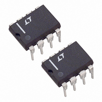
LT1173CN8-5 Linear Technology, LT1173CN8-5 Datasheet - Page 10

LT1173CN8-5
Manufacturer Part Number
LT1173CN8-5
Description
IC DC/DC CONV FIXED OUT 5V 8DIP
Manufacturer
Linear Technology
Type
Step-Down (Buck), Step-Up (Boost), Invertingr
Datasheet
1.LT1173CN8-5PBF.pdf
(16 pages)
Specifications of LT1173CN8-5
Internal Switch(s)
Yes
Synchronous Rectifier
No
Number Of Outputs
1
Voltage - Output
5V
Current - Output
400mA
Frequency - Switching
23kHz
Voltage - Input
2 ~ 30 V
Operating Temperature
0°C ~ 70°C
Mounting Type
Through Hole
Package / Case
8-DIP (0.300", 7.62mm)
Power - Output
500mW
Lead Free Status / RoHS Status
Contains lead / RoHS non-compliant
Available stocks
Company
Part Number
Manufacturer
Quantity
Price
Company:
Part Number:
LT1173CN8-5#PBF
Manufacturer:
LT
Quantity:
952
Part Number:
LT1173CN8-5#PBF
Manufacturer:
LINEAR/凌特
Quantity:
20 000
A
Using the I
The LT1173 switch can be programmed to turn off at a set
switch current, a feature not found on competing devices.
This enables the input to vary over a wide range without
exceeding the maximum switch rating or saturating the
inductor. Consider the case where analysis shows the
LT1173 must operate at an 800mA peak switch current
with a 2.0V input. If V
will rise to 1.6A, exceeding the maximum switch current
rating. With the proper resistor selected (see the “Maxi-
mum Switch Current vs R
current will be limited to 800mA, even if the input voltage
increases.
Another situation where the I
when the device goes into continuous mode operation.
This occurs in step-up mode when
When the input and output voltages satisfy this relation-
ship, inductor current does not go to zero during the
switch OFF time. When the switch turns on again, the
current ramp starts from the non-zero current level in the
inductor just prior to switch turn on. As shown in Figure
9, the inductor current increases to a high level before the
comparator turns off the oscillator. This high current can
cause excessive output ripple and requires oversizing the
output capacitor and inductor. With the I
however, the switch current turns off at a programmed
level as shown in Figure 10, keeping output ripple to a
minimum.
10
LT1 173
–V
PPLICATI
IN
V
OUT
+
V
IN
C2
Figure 8. Negative-to-Positive Converter
LIM
V
V
AO
DIODE
SW
GND
I
Pin
LIM
O
LT1173
U
IN
V
SW2
IN
S
1
SW1
rises to 4V, the peak switch current
FB
1
I FOR ATIO
LIM
DC
U
L1
” characteristic), the switch
LIM
.
feature is useful occurs
R2
W
D1
V
OUT
+
=
( )
R1
R2
C1
LIM
1.245V + 0.6V
U
2N3906
feature,
R1
LT1173 • TA13
+V
17
OUT
SWITCH
Figure 11 details current limit circuitry. Sense transistor
Q1, whose base and emitter are paralleled with power
switch Q2, is ratioed such that approximately 0.5% of Q2’s
collector current flows in Q1’s collector. This current is
passed through internal 80 resistor R1 and out through
the I
between I
cient switch current flows to develop a V
R
turning off the switch. Delay through this circuitry is
approximately 2 s. The current trip point becomes less
accurate for switch ON times less than 4 s. Resistor
values programming switch ON time for 2 s or less will
cause spurious response in the switch circuitry although
the device will still maintain output regulation.
SWITCH
Figure 10. Current Limit Keeps Inductor Current Under Control
LIM
LIM
, Q3 turns on and injects current into the oscillator,
OFF
ON
OFF
Figure 9. No Current Limit Causes Large Inductor
Current Build-Up
ON
I
L
I
L
pin. The value of the external resistor connected
LIM
Figure 11. LT1173 Current Limit Circuitry
PROGRAMMED CURRENT LIMIT
V
OSCILLATOR
IN
and V
Q3
IN
(EXTERNAL)
sets the current limit. When suffi-
DRIVER
R
LIM
I
LIM
Q1
R1
80
(INTERNAL)
SW1
LT1173 • TA28
Q2
BE
SW2
across R1 +
LT1173 • TA14
LT1173 • TA15


