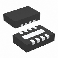
LTC3125EDCB#TRPBF Linear Technology, LTC3125EDCB#TRPBF Datasheet

LTC3125EDCB#TRPBF
Specifications of LTC3125EDCB#TRPBF
Available stocks
Related parts for LTC3125EDCB#TRPBF
LTC3125EDCB#TRPBF Summary of contents
Page 1
... Other features include a <1μA shutdown current, short- circuit and thermal overload protection. The LTC3125 is offered in a low profi le 0.75mm × 2mm × 3mm package. L, LT, LTC, LTM and Burst Mode are registered trademarks of Linear Technology Corporation. All other trademarks are the property of their respective owners. 100 ...
Page 2
... ORDER INFORMATION LEAD FREE FINISH TAPE AND REEL LTC3125EDCB#PBF LTC3125EDCB#TRPBF Consult LTC Marketing for parts specifi ed with wider operating temperature ranges. Consult LTC Marketing for information on non-standard lead based fi nish parts. For more information on lead free part marking, go to: For more information on tape and reel specifi ...
Page 3
ELECTRICAL CHARACTERISTICS junction temperature range, otherwise specifi cations are at T PARAMETER PROG Current Gain Maximum Duty Cycle Minimum Duty Cycle Frequency SHDN Input High SHDN Input Low SHDN Input Current Note 1: Stresses beyond those listed under Absolute Maximum ...
Page 4
LTC3125 TYPICAL PERFORMANCE CHARACTERISTICS Effi ciency vs Load Current OUT 100 3. 0.001 0.01 0.1 LOAD CURRENT (A) 3125 G03 ...
Page 5
TYPICAL PERFORMANCE CHARACTERISTICS DS(ON) OUT 0.450 0.400 0.350 0.300 PMOS 0.250 0.200 NMOS 0.150 0.100 0.050 1.5 2 2.5 3 3.5 4 4.5 V (V) OUT 3125 G12 Feedback vs Temperature 0.50 NORMALIZED TO 25°C 0.25 0 ...
Page 6
LTC3125 TYPICAL PERFORMANCE CHARACTERISTICS V and I During Soft-Start OUT IN V OUT 2V/DIV SHDN 5V/DIV INPUT CURRENT 200mA/DIV V = 3.3V 2s/DIV 4.5V OUT OUT L = 2.7μH PIN FUNCTIONS GND (Pin 1, ...
Page 7
BLOCK DIAGRAM PROG 3 R PROG SHDN 6 SHUTDOWN OSC THERMAL SHUTDOWN SENSE V BEST – ANTI-RING ...
Page 8
LTC3125 OPERATION The LTC3125 provides high effi ciency, low noise power for applications in portable instrumentation and those with pulsed-load, power-limited requirements such as GSM modems. The LTC3125 directly and accurately controls the average input current. The high effi ciency ...
Page 9
OPERATION prevents the inductor current from reversing in polarity, improving effi ciency at light loads. OSCILLATOR An internal oscillator sets the switching frequency to 1.6MHz. SHUTDOWN Shutdown of the boost converter is accomplished by pulling SHDN below 0.35V and enabled ...
Page 10
LTC3125 APPLICATIONS INFORMATION Burst Mode operation is inhibited during start-up and soft-start and until least 0.38V greater than V OUT GSM and GPRS modems have become a popular wire- less data transfer solution for use in notebook ...
Page 11
APPLICATIONS INFORMATION power losses compared to cheaper powdered iron types, improving effi ciency. The inductor should have low DCR (DC resistance of the windings) to reduce the I losses, and must be able to support the peak inductor current without ...
Page 12
LTC3125 APPLICATIONS INFORMATION AVERAGE INPUT ILIMIT PROGRAMMING RESISTOR SELECTION The input current limit is user programmable by selection of an external resistor important to locate PROG the resistor as close to the pin as possible to ...
Page 13
TYPICAL APPLICATIONS PC Card (3.3V/1000mA Maximum) 4.5V Output, GPRS, Class 10 Pulsed Load 2.7μ CARD OUT 3.3V ±10% 10μF 1000mA MAX LTC3125 CER SHDN OFF ON PROG FB GND 22.6k ...
Page 14
LTC3125 TYPICAL APPLICATIONS 2. 500mA MAX 14 Stacked Supercap Charger 2.2μ OUT 10μF LTC3125 CER SHDN 2.74M OFF ON PROG FB GND 1M 44.2k *TDK VLF4014ST-2R2M1R9 **PANASONIC EECHWOD306 Waveforms of Input ...
Page 15
TYPICAL APPLICATIONS 3.3V ±10% 300mA 500mA 3. with Selectable Input Current Limit 2.2μ OUT 10μF LTC3125 CER SHDN 3.2M OFF ON PROG FB GND 1M 44.2k 28.7k M1 3125 TA07a *TDK ...
Page 16
LTC3125 PACKAGE DESCRIPTION 3.50 ±0.05 2.10 ±0.05 RECOMMENDED SOLDER PAD PITCH AND DIMENSIONS APPLY SOLDER MASK TO AREAS THAT ARE NOT SOLDERED PIN 1 BAR TOP MARK (SEE NOTE 6) 0.200 REF 16 DCB Package 8-Lead Plastic DFN (2mm × ...
Page 17
... Added Average Input Limit Programming Resistor Selection section Updated Related Parts table Information furnished by Linear Technology Corporation is believed to be accurate and reliable. However, no responsibility is assumed for its use. Linear Technology Corporation makes no representa- tion that the interconnection of its circuits as described herein will not infringe on existing patent rights. (Pin 7) ...
Page 18
... I IN OUT(MAX 0.7V to 5.5V 5.25V OUT(MAX) : 0. 5.25V OUT(MAX 0. 5.25V, IN OUT(MAX) < 1μA, 2mm × 3mm DFN Package SD LT 1210 REV A • PRINTED IN USA © LINEAR TECHNOLOGY CORPORA TION 2008 = 10μ 45μ 7μA, = 9μ 12μ 12μ 30μA, 3125fa ...


