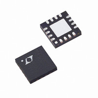
LT3582EUD-12#TRPBF Linear Technology, LT3582EUD-12#TRPBF Datasheet - Page 10

LT3582EUD-12#TRPBF
Manufacturer Part Number
LT3582EUD-12#TRPBF
Description
IC DC/DC CONV +/-12V 16-QFN
Manufacturer
Linear Technology
Type
Step-Up (Boost), Invertingr
Datasheet
1.LT3582EUDPBF.pdf
(28 pages)
Specifications of LT3582EUD-12#TRPBF
Internal Switch(s)
Yes
Synchronous Rectifier
No
Number Of Outputs
2
Voltage - Output
±12V
Current - Output
350mA, 600mA
Voltage - Input
2.55 ~ 5.5 V
Operating Temperature
-40°C ~ 125°C
Mounting Type
Surface Mount
Package / Case
16-WQFN Exposed Pad
Lead Free Status / RoHS Status
Lead free / RoHS Compliant
Power - Output
-
Frequency - Switching
-
Available stocks
Company
Part Number
Manufacturer
Quantity
Price
OPERATION
LT3582/LT3582-5/LT3582-12
The LT3582 series are dual DC/DC converters, each contain-
ing both a Boost and an Inverting converter. Operation can
be best understood by referring to the Block Diagram. The
Boost and Inverting converters each use a novel control
technique, which simultaneously varies both peak inductor
current and switch off time. This results in high effi ciency
over a large load range and low output voltage ripple. In
addition, this technique further minimizes output ripple
when the switching frequency is in the audio band.
Boost Converter: The Boost converter uses a grounded
source NMOS power transistor as the main switching ele-
ment. The current in the NMOS is constantly monitored and
controlled, along with the off-time of the switch to achieve
regulation of V
internal programmable (LT3582 only) resistor divider to
create FBP . The voltage on FBP is compared to an internal
reference and amplifi ed, creating an error signal on the
VCP node which commands the appropriate peak inductor
current and off time for the subsequent switching cycle.
Inverting Converter: The Inverting converter uses a power
PMOS transistor with the source connected to V
topology requires only one external inductor, instead of
the normally required two inductors plus fl ying capacitor.
Regulation is achieved in a similar manner as the Boost.
Output Power-Up Sequencing: After an initial start-up
delay (T
V
LT3582-12 or in one of four selectable sequences with
the LT3582. Using the I
10
OUTN
rise (in magnitude) simultaneously with the LT3582-5/
START-UP
OUTP
= 64μs typical), the outputs V
. The V
2
C interface, the LT3582 outputs
OUTP
voltage is divided by the
OUTP
IN
. This
and
can be confi gured such that (1) they both rise simultane-
ously, (2) V
V
output rises. The outputs of the LT3582-5 and LT3582-12
are pre-confi gured to rise simultaneously.
The ramp rates of the outputs are proportional to the ramp
rates of their respective RAMP pins. A capacitor is placed
between each RAMP pin and ground. The RAMP pins are
discharged during shutdown. Once enabled, confi gurable
(LT3582) or pre-confi gured (LT3582-5/LT3582-12) cur-
rents charge each RAMP pin in the desired sequence
causing the outputs to rise.
Output Power-Down Discharge: The power-down dis-
charge feature is permanently enabled on the LT3582-5
and LT3582-12 and can be enabled or disabled through
I
down discharge is enabled, internal transistors will acti-
vate to assist in discharging the outputs toward ground.
When power-down discharge is disabled, the chip powers
down immediately after SHDN falls and the outputs will
discharge on their own depending on their external load
capacitances and currents.
OTP Memory (LT3582 Only): The LT3582 includes 22 bits
of user programmable output settings and 1 programming
lockout bit. Parameters such as positive and negative output
voltages and power sequencing settings can be changed
in real time with the integrated I
then be made permanent by programming to the on-chip
non-volatile OTP (One Time Programmable) memory.
2
OUTN
C on the LT3582. Upon SHDN falling, and when power-
rises to regulation before V
OUTP
rises to regulation before V
2
C interface. Settings can
OUTP
rises, or (4) neither
OUTN
rises, (3)
3582512fb


