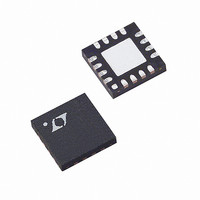
LT3582EUD-12#TRPBF Linear Technology, LT3582EUD-12#TRPBF Datasheet - Page 12

LT3582EUD-12#TRPBF
Manufacturer Part Number
LT3582EUD-12#TRPBF
Description
IC DC/DC CONV +/-12V 16-QFN
Manufacturer
Linear Technology
Type
Step-Up (Boost), Invertingr
Datasheet
1.LT3582EUDPBF.pdf
(28 pages)
Specifications of LT3582EUD-12#TRPBF
Internal Switch(s)
Yes
Synchronous Rectifier
No
Number Of Outputs
2
Voltage - Output
±12V
Current - Output
350mA, 600mA
Voltage - Input
2.55 ~ 5.5 V
Operating Temperature
-40°C ~ 125°C
Mounting Type
Surface Mount
Package / Case
16-WQFN Exposed Pad
Lead Free Status / RoHS Status
Lead free / RoHS Compliant
Power - Output
-
Frequency - Switching
-
Available stocks
Company
Part Number
Manufacturer
Quantity
Price
LT3582/LT3582-5/LT3582-12
APPLICATIONS INFORMATION
All data bytes can be read from their assigned register
addresses. Since they share the same register addresses,
reads of the OTP and REG data bytes are differentiated
by their corresponding RSEL (Register Select) bits in the
CMDR register. All data written to register addresses 0-2 is
stored in REGO-REG2. Regardless of the RSEL bits, OTP
bytes cannot be written directly. See the OTP Programming
section for more information.
Data Transfer Protocol
The LT3582 series supports 8-bit data transfers in the
transaction formats shown in Figures 2 and 3. Multiple
data bytes can only be transferred by issuing multiple
transactions.
Figure 2 shows the required format for writing a byte of
data to the LT3582 series. Again, the chip address depends
on the CA pin logic state.
A byte of data is read from the LT3582 series using the
format shown in Figure 3. This transaction requires four I
bytes to read one byte of chip data and must be repeated
for each subsequent byte of data that is read.
12
S
S
FROM MASTER TO SLAVE
FROM SLAVE TO MASTER
0110 001 OR
0110 001 OR
CHIP ADDR
CHIP ADDR
1000 101
1000 101
S
Figure 2. I
Figure 3. I
0110 001 OR
CHIP ADDR
1000 101
W
W
0
0
2
2
A
A
0
0
C Byte Write Transaction
C Byte Read Transaction
00000b2:b0
00000b2:b0
REG ADDR
REG ADDR
R
1
A: ACKNOWLEDGE (LOW)
A: NOT ACKNOWLEDGE (HIGH)
R: READ BIT (HIGH)
W WRITE BIT (LOW)
S: START CONDITION
P: STOP CONDITION
A
0
b7:b0
DATA
A
0
A
0
b7:b0
DATA
A
1
A
0
P
P
2
C
LT3582 Chip Confi guration
Settings such as output voltages and sequencing are
digitally programmable. The chip uses settings from either
the REG or OTP bytes, depending on the states of the
corresponding RSEL bits (0 for OTP and 1 for REG).
During shutdown the RSEL bits are reset low. As a result,
the initial confi guration comes from the OTP data bytes.
After power-up, the confi guration can be changed by writing
new settings to the appropriate REG data byte(s) then
setting the corresponding RSEL bit(s).
Finally, data in the REG bytes can be permanently
programmed to OTP by applying voltage to the V
and setting the WOTP bit in the Command Register. See
the OTP Programming section for more information.
LT3582-5/LT3582-12 Chip Confi guration
The LT3582-5/LT3582-12 are shipped from the factory with
the OTP memory pre-programmed and LOCKed which
prohibits subsequent changes to the confi guration. The
confi guration can still be read through the I
the RST and SWOFF bits of the CMDR register (described
later) are functional. The following sections describe the
various confi gurable features of the LT3582. The LT3582-5
and LT3582-12 are pre-confi gured as follows: V
are programmed for ±5V or ±12V respectively, LOCK = 1,
IRMP = 00, PDDIS = 1, PUSEQ = 11 and V
or 0. Since LOCK = 1, subsequent confi guration changes
are prohibited. See Confi guration Lockout (LOCK Bit) for
more information.
Registers and OTP
The registers and OTP bytes for the LT3582 series are
organized as shown in Table 1. The CMDR is reset to 00h
upon power-up, during shutdown and during undervoltage
and thermal lockouts. REG0-REG2 are never reset and must
always be loaded with valid data before use. The LT3582’s
OTP memory is shipped with all 0’s, and as a result, the
PUSEQ bits are confi gured to disable the outputs. The
PUSEQ bits must be reconfi gured to enable the outputs.
PLUS
2
C bus and
may be 1
P
and V
3582512fb
PP
pin
N


