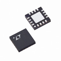
LT3582EUD-5#TRPBF Linear Technology, LT3582EUD-5#TRPBF Datasheet - Page 11

LT3582EUD-5#TRPBF
Manufacturer Part Number
LT3582EUD-5#TRPBF
Description
IC DC/DC CONV +/-5V 16-QFN
Manufacturer
Linear Technology
Type
Step-Up (Boost), Invertingr
Datasheet
1.LT3582EUDPBF.pdf
(28 pages)
Specifications of LT3582EUD-5#TRPBF
Internal Switch(s)
Yes
Synchronous Rectifier
No
Number Of Outputs
2
Voltage - Output
±5V
Current - Output
350mA, 600mA
Voltage - Input
2.55 ~ 5.5 V
Operating Temperature
-40°C ~ 125°C
Mounting Type
Surface Mount
Package / Case
16-WQFN Exposed Pad
Lead Free Status / RoHS Status
Lead free / RoHS Compliant
Power - Output
-
Frequency - Switching
-
Available stocks
Company
Part Number
Manufacturer
Quantity
Price
APPLICATIONS INFORMATION
I
The LT3582 series contains an I
allowing it to be digitally confi gured. The use of this interface
is optional for the LT3582-5 and LT3582-12 as these parts
are pre-confi gured at the factory. The CA, SDA and SCL
pins can be grounded if the I
The I
allow for direct communication with low voltage digital
ICs (see Electrical Characteristics). I
is disabled when SHDN is low. After SHDN rises, I
communication is re-enabled after a delay of 64μs (typical).
The chip is a read-write slave device which allows the user
to read the current settings and, for the LT3582, write
new ones. Most settings can be made permanent via the
One-Time-Programmable memory. The chip will always
enable using the data stored in OTP and the LT3582 can
be reconfi gured after power-up.
START and STOP Conditions
When the bus is idle, both SCL and SDA are high. A bus
master signals the beginning of a transmission with a START
condition by transitioning SDA from high to low while SCL
is high, as shown in Figure 1. When the master has fi nished
communicating with the slave, it issues a STOP condition
by transitioning SDA from low to high while SCL is high.
The bus is then free for another transmission.
2
C Interface
2
C interface has reduced input threshold voltages to
SDA
SCL
CONDITION
START
S
ADDRESS
CHIP
A6 - A0
1-7
2
C interface is unused.
2
C compatible interface
R/W
8
2
C communication
ACK
9
Figure 1. Data Transfer Over I
1-7
B7 - B0
DATA
2
C
8
ACKnowledge
The acknowledge signal (ACK) is used in handshaking
between transmitter and receiver to indicate that the most
recent byte of data was received. The transmitter always
releases the SDA line during the acknowledge clock pulse.
When the slave is the receiver, it pulls down the SDA line
so that it remains LOW during this pulse to acknowledge
receipt of the data. If the slave fails to acknowledge
by leaving SDA high, then the master may abort the
transmission by generating a STOP condition. When the
master is receiving data from the slave, the master pulls
down the SDA line during the clock pulse to indicate receipt
of the data. After the last byte has been received the master
leaves the SDA line HIGH (not acknowledge) and issues a
stop condition to terminate the transmission.
Device Addressing
The LT3582 series supports two 7-bit chip addresses
depending on the logic state of the CA pin. The addresses
are 0110 001 (CA = 1) and 1000 101 (CA = 0). Also, there
are seven internal data byte locations as shown in Table 1.
OTP0-OTP2 are the OTP memory bytes. REG0-REG2
are the corresponding volatile registers used for storing
alternate settings. Finally, the Command Register (CMDR)
is used for additional control of the chip.
LT3582/LT3582-5/LT3582-12
ACK
9
2
C Bus
1-7
B7 - B0
DATA
8
ACK
9
CONDITION
STOP
3582512 F01
P
11
3582512fb


