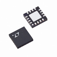
LT3582EUD-5#TRPBF Linear Technology, LT3582EUD-5#TRPBF Datasheet - Page 15

LT3582EUD-5#TRPBF
Manufacturer Part Number
LT3582EUD-5#TRPBF
Description
IC DC/DC CONV +/-5V 16-QFN
Manufacturer
Linear Technology
Type
Step-Up (Boost), Invertingr
Datasheet
1.LT3582EUDPBF.pdf
(28 pages)
Specifications of LT3582EUD-5#TRPBF
Internal Switch(s)
Yes
Synchronous Rectifier
No
Number Of Outputs
2
Voltage - Output
±5V
Current - Output
350mA, 600mA
Voltage - Input
2.55 ~ 5.5 V
Operating Temperature
-40°C ~ 125°C
Mounting Type
Surface Mount
Package / Case
16-WQFN Exposed Pad
Lead Free Status / RoHS Status
Lead free / RoHS Compliant
Power - Output
-
Frequency - Switching
-
Available stocks
Company
Part Number
Manufacturer
Quantity
Price
APPLICATIONS INFORMATION
several start-up issues have occurred: A) the expected
V
ringing occurs C) the V
the output disconnect current limit being reached D) ad-
ditional ringing occurs when the CAPP pin starts charging
E) output voltage overshoot occurs because the inductor
currents are maximized during the output ramp-up.
In some cases it may be desirable to use only one RAMP
pin capacitor. In cases where PUSEQ = 11 (see the Power-
Up Sequencing section) the RAMPP and RAMPN pins
can be connected together and to a single capacitor. In
this case the capacitor will charge with twice the current
confi gured by the IRMP bits.
Ramping V
the unique ability to generate a smooth V
ramp starting from ground and continuing all the way up
to regulation (see Figure 6). This ability is not possible
with typical Boost converters in which the output is taken
from the cathode of the Schottky diode (CAPP node in
Figure 5).
OUTP
V
IN
0.2V/DIV
0.2A/DIV
ramp up path is not followed B) inductor current
V
Figure 6. V
2V/DIV
2V/DIV
RAMPP
V
CAPP
C1
OUTP
I
L2
L1
OUTP
SWP
Figure 5. Boost Converter Topology
OUTP
from Ground: The LT3582 series has
D1
C2
Soft-Start Ramping from Ground
CAPP
OUTP
1ms/DIV
ramp rate is limited due to
DISCONNECT
CONTROL
LT3582
SERIES
3582512 F06
OUTP
C3
LOAD
voltage
3582512 F05
V
OUTP
The LT3582 series incorporates an output disconnect
PMOS allowing V
Once enabled, the Disconnect Control circuit actively
drives the PMOS gate allowing V
as shown in Figure 6. Once V
the PMOS is fully turned “on” to reduce resistance and
improve effi ciency.
Power-Up Sequencing (PUSEQ bits)
Once enabled, the part requires a delay of T
typ) to properly confi gure itself. Once confi gured, the order
in which V
by the PUSEQ bits. The combinations available for the
LT3582 are shown in Table 2. The LT3582-5/LT3582-12
are pre-confi gured with the 11 combination.
Table 2. Power-Up Sequences
Selecting the 01 or 10 combinations cause one of the out-
puts to start ramping shortly after SHDN rises. The ramp
rate of V
in the Soft-Start section. After V
PUSEQ[1:0] Power-Up Sequence
LT3582/LT3582-5/LT3582-12
00
01
10
11
Figure 7. V
0.2A/DIV
0.5V/DIV
V
3V/DIV
3V/DIV
OUT
RAMPP
V
CAPP
OUTP
OUTP
I
L2
Outputs are disabled, neither output ramps up
V
V
Both V
is controlled by the RAMP pin as discussed
OUTN
OUTP
B
and V
OUTP
ramps up 1st, followed by V
ramps up 1st, followed by V
OUTP
OUTP
Soft-Start with Excessive Ramp Rate
C
OUTN
D
and V
to be grounded during shutdown.
A
50μs/DIV
OUTN
ramp to regulation is controlled
ramp-up starting at the same time.
OUT
OUTP
E
OUTP
nears its target regula-
reaches regulation,
to ramp up linearly
OUTP
OUTN
3582512 F07
START-UP
15
3582512fb
(64μs


